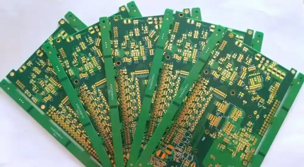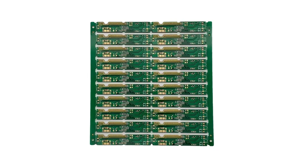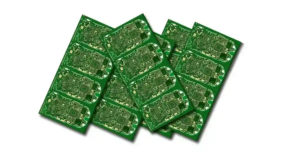
The evolution of electronic devices toward greater miniaturization and enhanced functionality has driven the widespread adoption of multilayer PCBs across industries. These sophisticated circuit boards represent a fundamental advancement in electronic design, enabling the creation of compact, high-performance devices that power everything from smartphones to aerospace systems.
Multilayer PCBs are printed circuit boards containing three or more conductive layers, with interconnected copper traces separated by insulating substrate materials. Unlike single or double-sided boards, multilayer PCBs provide superior routing density, improved electromagnetic interference (EMI) shielding, and enhanced signal integrity through their advanced stackup configurations.
Understanding Multilayer PCB Architecture
Core Construction Principles
Multilayer PCBs feature a sophisticated laminated structure consisting of alternating conductive copper layers and insulating dielectric materials. The manufacturing process involves precise lamination of prepreg (pre-impregnated) materials with copper foil under controlled temperature and pressure conditions. This results in a unified board structure where internal layers are completely enclosed within the substrate.
The fundamental architecture typically includes dedicated power and ground planes positioned strategically within the stackup to optimize power distribution and minimize electromagnetic emissions. Signal routing layers are positioned adjacent to these reference planes to maintain controlled impedance characteristics essential for high-speed digital applications.
Layer Count Considerations
Modern multilayer PCBs range from four-layer configurations for basic applications to complex designs exceeding 40 layers for advanced systems. The selection of layer count depends on routing density requirements, signal integrity considerations, and cost constraints. Industry standards typically favor even-numbered layer counts due to manufacturing efficiency and structural symmetry, which prevents board warpage during the lamination process.
Common layer configurations include:
| Layer Count | Typical Applications | Key Benefits |
|---|---|---|
| 4-6 layers | Consumer electronics, basic digital devices | Cost-effective, adequate routing density |
| 8-12 layers | Smartphones, tablets, networking equipment | Enhanced signal integrity, compact form factor |
| 14-20 layers | High-performance computing, telecommunications | Superior EMI control, complex routing capability |
| 20+ layers | Advanced aerospace, military systems | Maximum functionality, extreme miniaturization |
Via Technology and Interconnection Methods
Multilayer PCBs utilize three primary via technologies to establish connections between layers. Through-hole vias penetrate the entire board thickness, connecting outer layers to any internal layer. These represent the most cost-effective interconnection method and are suitable for standard applications requiring robust electrical connections.
Blind vias connect outer layers to specific internal layers without penetrating the complete board thickness. This technology enables higher routing density by preserving board real estate while providing necessary interconnections. Buried vias connect internal layers exclusively, remaining invisible from the board surface and maximizing component placement density.
Advanced Via Structures
Modern multilayer PCB designs increasingly employ microvias with diameters typically ranging from 0.1mm to 0.15mm. These high-density interconnection (HDI) structures enable fine-pitch component mounting and support the miniaturization demands of portable electronics. Stacked and staggered via configurations provide additional routing flexibility while maintaining signal integrity in complex designs.
Stackup Design and Signal Integrity
Optimal Layer Arrangement
Effective multilayer PCB design requires careful consideration of layer stackup to achieve desired electrical performance. The arrangement of signal layers relative to reference planes directly impacts impedance control, crosstalk mitigation, and electromagnetic compatibility. Industry best practices recommend positioning high-speed signal layers adjacent to solid reference planes with minimal dielectric thickness.
Impedance Control Strategies
Controlled impedance design ensures reliable signal transmission in multilayer PCBs. Single-ended traces typically target 50-ohm impedance, while differential pairs are designed for 100-ohm impedance characteristics. The dielectric constant of substrate materials, trace geometry, and layer spacing collectively determine impedance values, requiring precise calculation and validation during the design phase.
Power distribution networks within multilayer PCBs benefit from dedicated power and ground planes that provide low-impedance current paths and effective decoupling. The separation between power and ground planes creates a distributed capacitance that helps filter high-frequency noise and maintain stable power delivery to active components.

Manufacturing Processes and Quality Control
Lamination Technology
Multilayer PCB manufacturing employs sophisticated lamination processes using hydraulic presses operating at temperatures exceeding 180°C and pressures reaching 400 PSI. The lamination cycle duration and cooling profile are precisely controlled to ensure complete resin cure while preventing delamination or void formation between layers.
Drilling and Plating Operations
Precision drilling operations create via holes using computer-controlled equipment capable of achieving positional accuracies within ±0.05mm. Subsequent electroplating processes deposit copper within via barrels to establish reliable electrical connections. Advanced plating chemistry and process controls ensure uniform copper distribution and adequate thickness for long-term reliability.
Applications Across Industries
Consumer Electronics Integration
Multilayer PCBs enable the compact designs essential for modern consumer electronics. Smartphones typically employ 8-12 layer configurations to accommodate complex circuitry including processors, memory, radio frequency components, and power management systems within minimal form factors. The superior EMI shielding properties of multilayer designs help meet regulatory compliance requirements while maintaining device performance.
Telecommunications Infrastructure
Network infrastructure equipment relies on multilayer PCBs for high-speed data processing and transmission capabilities. These applications demand exceptional signal integrity performance and the ability to handle multiple gigabit data streams simultaneously. The controlled impedance characteristics and low insertion loss properties of multilayer designs make them ideal for such demanding applications.
Automotive and Aerospace Systems
The automotive industry increasingly adopts multilayer PCBs for advanced driver assistance systems, engine control units, and infotainment systems. These applications require boards capable of operating reliably in harsh environmental conditions while maintaining precise electrical performance. Aerospace applications demand even higher reliability standards, often requiring specialized materials and manufacturing processes to meet stringent qualification requirements.

Design Considerations and Best Practices
Electromagnetic Compatibility
Multilayer PCB design must address electromagnetic compatibility requirements through proper stackup selection and component placement strategies. Ground planes provide effective shielding while maintaining low-impedance return paths for high-frequency currents. Strategic placement of decoupling capacitors and careful routing of sensitive signals help minimize electromagnetic emissions and improve immunity to external interference.
Thermal Management
Advanced multilayer designs incorporate thermal management features including thermal vias, copper-filled areas, and specialized substrates with enhanced thermal conductivity. These features help dissipate heat generated by high-power components while maintaining electrical performance and long-term reliability.
Partner with Haoyue Electronics for Your Multilayer PCB Needs
At Haoyue Electronics, we specialize in the design and manufacturing of high-quality multilayer PCBs tailored to meet the demanding requirements of modern electronic applications. Our advanced manufacturing capabilities include support for layer counts ranging from 4 to 32 layers, with precision drilling, controlled impedance design, and comprehensive quality assurance testing.
Our experienced engineering team provides comprehensive design for manufacturing (DFM) support to optimize your multilayer PCB designs for cost-effectiveness and reliability. From prototype development to high-volume production, we deliver consistent quality and competitive lead times. Contact our technical team today to discuss your multilayer PCB requirements and discover how our expertise can accelerate your product development timeline while ensuring superior performance and reliability.
FAQ
1. What are the advantages of using multilayer PCBs in electronics design?
Multilayer PCBs offer several key advantages, including higher routing density, improved signal integrity, and superior EMI shielding. These advantages make multilayer PCBs ideal for compact, high-performance devices such as smartphones, computers, and aerospace systems. By incorporating multiple conductive layers, multilayer PCBs enable the design of more sophisticated and reliable electronics.
2. How do I choose the right layer count for my multilayer PCB design?
The number of layers in a multilayer PCB depends on several factors such as routing density, signal integrity requirements, and cost constraints. For example, 4-6 layer PCBs are common for consumer electronics, while 8-12 layer PCBs are often used in devices like smartphones. For high-performance applications like telecommunications and aerospace, designs may require 20+ layers. It’s essential to balance performance needs with manufacturing capabilities.
3. What is impedance control, and why is it important in multilayer PCB design?
Impedance control ensures that signal transmission in a multilayer PCB is reliable and stable. By carefully controlling the impedance of single-ended traces (typically 50Ω) and differential pairs (usually 100Ω), designers can minimize signal reflection and loss. Proper impedance control is particularly important in high-speed and high-frequency applications, ensuring signal integrity in advanced electronic systems.
4. What are the common via technologies used in multilayer PCBs?
Multilayer PCBs employ several via types, including through-hole vias, blind vias, and buried vias. Through-hole vias connect outer layers to internal layers, making them cost-effective for standard designs. Blind vias connect outer layers to specific internal layers, while buried vias are used for internal layer interconnections only, maximizing board real estate. For high-density interconnections (HDI), microvias are increasingly used for miniaturized designs.
5. What industries use multilayer PCBs, and what are their key applications?
Multilayer PCBs are used across a wide range of industries, including consumer electronics, telecommunications, automotive, and aerospace. They are essential in smartphones, network infrastructure equipment, driver assistance systems (ADAS), and military and aerospace electronics, where compactness, reliability, and high performance are critical. The ability to handle complex routing and maintain signal integrity makes multilayer PCBs indispensable for these applications.

