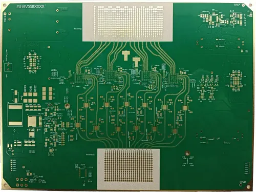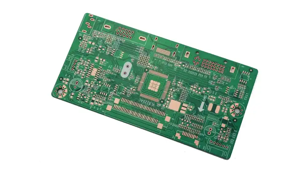
High Frequency Printed Circuit Boards (HF PCBs) represent a critical advancement in modern electronics, specifically engineered to handle signals operating at frequencies above 1 GHz. These specialized circuit boards have become indispensable in today’s technology landscape, where wireless communication, 5G networks, satellite systems, and advanced medical devices demand superior signal integrity and minimal transmission losses.
Unlike conventional PCBs that utilize standard FR4 materials, High Frequency PCBs employ advanced substrate materials such as PTFE (Teflon), Rogers laminates, and other low-loss dielectric materials. This fundamental difference enables HF PCBs to maintain signal quality at frequencies ranging from 500 MHz to over 20 GHz, making them essential for applications requiring high-speed data transmission and precise signal control.
Understanding High Frequency PCB Technology
Frequency Range and Applications
High Frequency PCBs operate effectively across a broad spectrum, typically handling frequencies from 500 MHz to beyond 20 GHz. This extensive range encompasses various critical applications including microwave communications, millimeter-wave radar systems, and emerging 6G wireless technologies. The definition of “high frequency” continues to evolve with technological advancement, but any application requiring frequencies above 1 GHz generally necessitates specialized HF PCB design considerations.
Key Differentiators from Standard PCBs
The primary distinction between High Frequency PCBs and conventional boards lies in their material composition and design complexity. Standard PCBs rely on FR4 substrates with glass transition temperatures around 130-140°C, while HF PCBs utilize advanced materials with superior electrical properties. These specialized substrates exhibit lower dielectric constants, reduced loss tangents, and enhanced thermal stability, enabling them to maintain signal integrity at elevated frequencies where standard materials would introduce unacceptable losses.
Essential Material Properties for High Frequency PCBs
Dielectric Constant and Loss Tangent
The selection of appropriate dielectric materials forms the foundation of effective HF PCB design. The dielectric constant (Dk) determines signal propagation speed and impedance characteristics, while the dissipation factor (Df) or loss tangent directly impacts signal attenuation. Optimal HF PCB materials exhibit low and stable Dk values, typically ranging from 2.2 to 4.5, combined with minimal loss tangents below 0.004 at operating frequencies.
Advanced Substrate Materials
Rogers materials represent the industry standard for high-performance HF PCBs, offering exceptional electrical properties and thermal stability. Rogers RO4350B provides a balanced combination of performance and processability with a Dk of 3.48 and Df of 0.0037 at 10 GHz. For ultra-low loss applications, Rogers RO3003 delivers superior performance with a Dk of 3.0 and Df of 0.0013, making it ideal for millimeter-wave applications.
PTFE-based materials offer the lowest dielectric losses but require specialized processing techniques. Taconic TLX and TLC series provide excellent electrical performance for demanding microwave applications, while ARLON materials offer high-temperature stability for automotive and aerospace applications.
Copper Foil Technology
The copper conductor system significantly influences HF PCB performance, particularly at frequencies above 2.4 GHz where skin effect losses become pronounced. Modern HF PCBs utilize specialized copper foils designed to minimize surface roughness and reduce conductor losses.
| Copper Foil Type | Surface Roughness | Primary Applications |
|---|---|---|
| Ultra-Low Profile (ULP) | <0.3 μm | >10 GHz applications |
| Very Low Profile (VLP) | 0.3–0.5 μm | 2–10 GHz applications |
| Reverse Treated Foil (RTF) | 0.5–1.5 μm | General HF applications |
| Standard Electrodeposited | >1.0 μm | Lower frequency applications |
Design Considerations for High Frequency PCBs
Impedance Control and Signal Integrity
Maintaining precise impedance control represents a fundamental requirement in HF PCB design. Signal integrity depends on consistent characteristic impedance throughout the transmission path, typically standardized at 50 ohms for single-ended signals or 100 ohms for differential pairs. This requires careful control of trace geometry, dielectric thickness, and substrate properties.
Thermal Management Strategies
High Frequency PCBs generate significant heat due to increased power densities and dielectric losses at elevated frequencies. Effective thermal management incorporates multiple strategies including thermal vias for heat dissipation, copper pour areas for heat spreading, and careful component placement to minimize thermal hotspots. The thermal coefficient of dielectric constant (TCDk) becomes critical, as temperature variations can shift circuit performance and degrade signal quality.
Via Design and Layer Stack-up
Via structures in HF PCBs require specialized design approaches to minimize discontinuities and parasitic effects. Blind and buried vias reduce signal path lengths and eliminate unnecessary layer transitions, while via stitching techniques improve return current paths and reduce ground plane resonances. Optimal layer stack-up design maintains controlled impedance while providing adequate isolation between signal layers.
Manufacturing Excellence in High Frequency PCBs
Precision Manufacturing Requirements
Manufacturing High Frequency PCBs demands exceptional precision and process control throughout the fabrication sequence. Critical parameters include etching accuracy within ±10% of nominal dimensions, drilling precision with positional tolerances of ±0.05mm, and plating thickness uniformity to maintain impedance consistency. Advanced manufacturing facilities employ statistical process control to ensure consistent results across production batches.
Quality Assurance and Testing
Comprehensive testing protocols validate HF PCB performance across multiple parameters. Time Domain Reflectometry (TDR) measurements verify impedance control and identify discontinuities, while Vector Network Analyzer (VNA) testing characterizes insertion loss and return loss performance. Thermal cycling tests ensure reliability under operational temperature ranges, while microsection analysis verifies internal construction quality.
Advanced Manufacturing Technologies
Modern HF PCB fabrication utilizes sophisticated equipment and processes including Laser Direct Imaging (LDI) for precise pattern definition, plasma desmear processes for optimal via reliability, and controlled atmosphere processing to prevent contamination. Sequential lamination techniques enable complex multilayer constructions while maintaining excellent electrical performance.
Related Post
Challenges in High Frequency PCB Manufacturing

Industry Applications and Market Drivers
Telecommunications Infrastructure
The deployment of 5G networks and advancement toward 6G technologies drives significant demand for High Frequency PCBs. Base station equipment, massive MIMO antenna systems, and millimeter-wave communication devices all require HF PCBs capable of handling frequencies from 24 GHz to beyond 100 GHz. These applications demand exceptional phase stability and minimal insertion loss to maintain signal quality across extended transmission distances.
Aerospace and Defense Systems
Military radar systems, satellite communication equipment, and electronic warfare platforms utilize HF PCBs for their superior performance characteristics. These applications often require operation under extreme environmental conditions, necessitating materials and designs capable of maintaining performance across wide temperature ranges while withstanding mechanical stress and vibration.
Automotive Electronics Revolution
Advanced Driver Assistance Systems (ADAS) and autonomous vehicle technologies increasingly rely on High Frequency PCBs for radar-based sensing systems. Automotive radar operating at 24 GHz and 77 GHz frequencies requires HF PCBs that can maintain accuracy and reliability under harsh automotive environments while meeting stringent cost targets for volume production.
Medical Device Innovation
High-resolution medical imaging systems, including MRI, CT, and ultrasound equipment, utilize HF PCBs to process and transmit high-frequency signals with exceptional fidelity. These applications demand ultra-low noise performance and precise signal timing to achieve optimal image quality and diagnostic accuracy.
Related Post
High Frequency PCB Applications and Advantages
Future Trends and Technology Evolution
The High Frequency PCB industry continues evolving to meet increasing performance demands. Emerging trends include the development of ultra-low loss materials for millimeter-wave applications, advanced packaging technologies integrating HF PCBs with semiconductor devices, and additive manufacturing techniques enabling complex three-dimensional RF structures.
Environmental sustainability considerations are driving the development of halogen-free HF PCB materials and recyclable substrate options. Additionally, artificial intelligence and machine learning applications in design optimization are enabling more efficient HF PCB development processes and improved performance prediction capabilities.
Partner with Haoyue Electronics for Your High Frequency PCB Needs
At Haoyue Electronics, we understand the critical importance of precision and reliability in High Frequency PCB manufacturing. Our state-of-the-art facility combines advanced manufacturing technologies with rigorous quality control processes to deliver HF PCBs that meet the most demanding specifications.
Our engineering team possesses extensive experience in HF PCB design optimization, material selection, and manufacturing process development. We work closely with our clients to ensure optimal performance for their specific applications, whether in telecommunications, aerospace, automotive, or medical device sectors.
From prototype development through high-volume production, Haoyue Electronics provides comprehensive PCB manufacturing and assembly services tailored to High Frequency applications. Contact our technical team today to discuss how we can support your next HF PCB project with proven expertise and reliable delivery.

