Understanding HDI PCB Technology
What Defines an HDI PCB
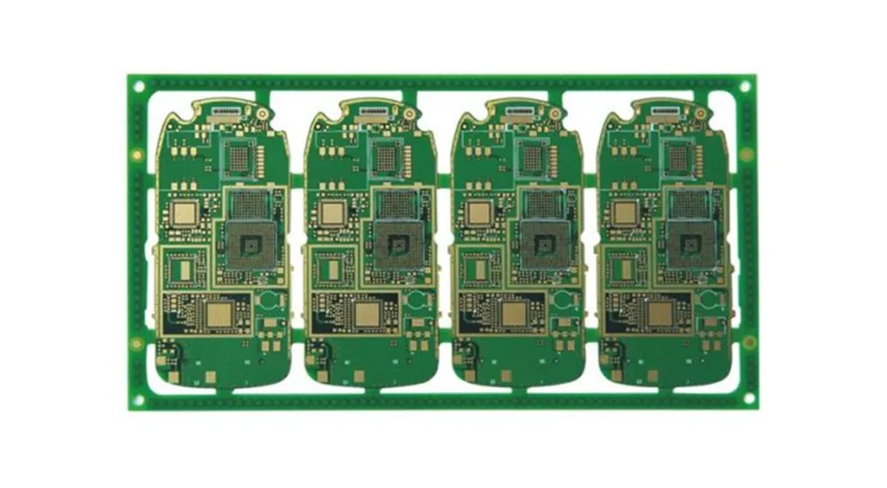
HDI PCB stands for High Density Interconnect Printed Circuit Board. These boards achieve significantly higher wiring density per unit area compared to conventional PCBs through advanced manufacturing techniques. The technology employs microvias, fine-line traces, and sequential build-up processes to create interconnect structures that would be impossible with traditional PCB manufacturing methods.
The key distinction lies in the approach to layer construction. Rather than manufacturing all layers simultaneously, HDI boards build up additional layers sequentially, allowing for more precise control over interconnect placement and enabling complex routing schemes. This methodology supports component densities and electrical performance levels that conventional PCB technology cannot achieve.
If you’d like to explore more about the differences between HDI PCB and standard PCB technologies, please refer to our detailed comparison article: HDI PCB vs Standard PCB | 6 Critical Differences.
Core HDI Technologies
HDI construction relies on several fundamental technologies working in concert:
- Microvias: Measuring between 0.05mm and 0.15mm in diameter, these provide precise connections between adjacent layers. Laser-drilled with exceptional accuracy, they enable placement densities far exceeding conventional mechanical drilling capabilities.
- Sequential lamination: Forms the backbone of HDI manufacturing, where each build-up layer undergoes a complete fabrication cycle including drilling, plating, and patterning before the next layer addition. This methodical approach ensures dimensional accuracy and electrical performance throughout increasingly complex stack-ups.
- Fine-line technology: Enables trace widths and spacing below 0.1mm, dramatically increasing routing density. Combined with controlled impedance design, these fine features maintain signal integrity even in electrically dense environments.
HDI PCB Architecture and Construction Methods
Layer Stack-up Design
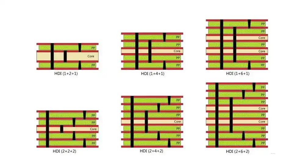
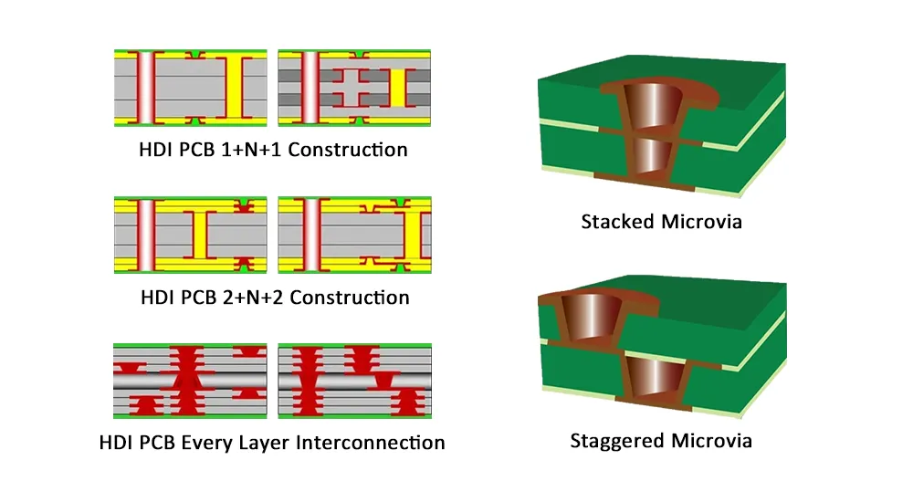
HDI boards employ various layer stack-up configurations to meet specific application requirements:
- Type I HDI: The simplest configuration, featuring microvias connecting surface layers to the first buried layer.
- Type II HDI: Incorporates stacked microvias extending through multiple build-up layers.
- Type III and higher: Include staggered microvias and buried via structures for maximum routing flexibility.
The choice of stack-up configuration depends on signal routing requirements, component density, and performance specifications. Higher-type HDI constructions enable greater routing flexibility but require more sophisticated manufacturing processes and typically command higher costs.
Each layer in an HDI stack-up serves specific functions. Core layers provide mechanical stability and accommodate high-current power distribution. Build-up layers handle fine-pitch component connections and high-speed signal routing. The sequential nature of HDI construction allows engineers to optimize each layer for its intended function.
Advanced Via Technologies
Modern HDI fabrication incorporates multiple via technologies to achieve optimal interconnect performance:
- Laser-drilled microvias: Offer precise positioning and minimal thermal stress compared to mechanical drilling. These microvias can be filled with conductive materials to improve reliability and enable stacking of additional layers.
- Buried vias: Connect internal layers without consuming surface routing space, maximizing available area for component placement.
- Skip vias: Span multiple layers in a single structure, reducing via count and improving signal integrity for high-speed applications.
The combination of these via technologies creates three-dimensional interconnect networks that efficiently utilize available board space. This capability proves particularly valuable in applications requiring high component density or complex signal routing schemes.
Applications Across Industries
Consumer Electronics
The consumer electronics sector drives much of the innovation in HDI technology. Smartphones represent perhaps the most demanding application, requiring integration of powerful processors, memory subsystems, wireless communication circuits, and power management systems within extremely compact form factors.
Modern smartphones typically employ HDI constructions ranging from 8 to 16 layers, incorporating multiple build-up layers on both sides of a thin core. These designs accommodate fine-pitch ball grid array processors, high-density memory packages, and numerous passive components while maintaining the thin profiles consumers expect.
Wearable devices present even greater miniaturization challenges. Smartwatches, fitness trackers, and hearing aids rely on HDI technology to integrate complex electronics within severely space-constrained packages. The technology enables these devices to offer sophisticated functionality while maintaining comfortable form factors.
Automotive Electronics
The automotive industry increasingly adopts HDI technology for advanced driver assistance systems, infotainment platforms, and electric vehicle control modules. These applications demand high reliability under extreme operating conditions while meeting strict size and weight requirements.
Modern vehicles incorporate dozens of electronic control units, many of which benefit from HDI construction. Engine management systems, transmission controllers, and safety systems require the high component density and signal integrity that HDI technology provides. The automotive industry’s move toward electric and autonomous vehicles continues to drive demand for more sophisticated HDI implementations.
High-Performance Computing and Telecommunications
Data centers and telecommunications infrastructure represent another major application area for HDI technology. High-performance processors and memory subsystems require the interconnect density that only HDI construction can provide. These applications often employ the most advanced HDI constructions available, including Type III and higher classifications with complex buried via networks.
Network switches, routers, and wireless base stations utilize HDI technology to achieve the port density and signal integrity required for modern communication standards. The ongoing deployment of 5G networks drives demand for even more sophisticated HDI implementations capable of handling millimeter-wave frequencies and high-speed digital interfaces.
Manufacturing Processes and Considerations
Sequential Build-up Manufacturing
HDI manufacturing begins with conventional PCB processing for the core substrate, followed by sequential addition of build-up layers. Each build-up cycle includes several critical steps:
- Dielectric application: Precise coating of insulating materials between conductive layers.
- Laser drilling: Creating microvias with exceptional precision, typically achieving positional tolerances within ±0.025mm.
- Desmear processing: Removing drilling debris and preparing via walls for reliable plating adhesion.
- Copper plating: Multiple plating steps to achieve specified copper thickness while maintaining via fill quality.
This iterative approach requires precise process control to maintain dimensional accuracy and electrical performance. The laser parameters must be carefully optimized for each dielectric material to ensure clean via formation without thermal damage to surrounding structures.
Quality Control and Testing
HDI manufacturing demands rigorous quality control throughout the fabrication process. Automated optical inspection systems verify via formation, trace geometry, and layer registration at each process step. Any defects discovered during intermediate inspections can often be corrected before proceeding to subsequent layers.
Electrical testing validates continuity, insulation resistance, and impedance characteristics across all interconnect structures. Cross-sectional analysis provides detailed verification of via formation quality and layer-to-layer adhesion. These testing methods ensure that finished HDI boards meet specification requirements and reliability standards.
Cost Factors and Economic Considerations
Understanding HDI Costs
HDI PCB cost reflects the sophisticated manufacturing processes and specialized equipment required for production. Several key factors drive pricing considerations:
- Sequential lamination complexity: Significantly increases processing time compared to conventional PCB fabrication, with each additional build-up layer requiring material, processing time, and yield considerations.
- Laser drilling equipment: Represents substantial capital investment that must be amortized across production volumes.
- Specialized materials and processes: Advanced dielectric materials and precise process control add complexity to the manufacturing workflow.
- Design complexity: Fine-line features, tight tolerances, and advanced materials all contribute to higher manufacturing costs.
- Via complexity: Stacked and buried structures influence pricing through increased process steps and potential yield impacts.
However, the functional benefits often justify these cost premiums in applications where HDI technology enables significant size reduction or performance improvement.
Design for Cost Optimization
Effective cost management begins during the design phase. Selecting appropriate HDI types for specific routing requirements avoids over-engineering while meeting performance objectives. Standardizing via structures and maintaining consistent design rules across different regions of the board helps control manufacturing complexity.
Early collaboration between design teams and manufacturing partners identifies potential cost reduction opportunities without compromising performance. Volume considerations play a crucial role in HDI economics, with higher production quantities enabling better material pricing and setup cost amortization.
Design Challenges and Best Practices
Signal Integrity Considerations
HDI design requires careful attention to signal integrity as trace densities increase and layer spacing decreases. Crosstalk between adjacent traces becomes more significant in HDI constructions, requiring advanced simulation tools and design techniques to maintain signal quality.
Power distribution presents unique challenges in HDI designs. The higher component densities and increased current requirements must be balanced against available copper area and thermal dissipation capabilities.
Effective power distribution design often requires multiple power planes and careful via placement to minimize resistance and inductance.
Thermal management becomes increasingly critical as component densities increase. HDI boards must dissipate heat efficiently while maintaining electrical performance. This requirement often drives material selection and may require specialized thermal management techniques such as embedded heat spreaders or thermal vias.
Design Rule Considerations
HDI design rules differ significantly from conventional PCB guidelines. Minimum via sizes, aspect ratios, and spacing requirements reflect the capabilities and limitations of HDI manufacturing processes. Design teams must understand these constraints to create manufacturable designs that meet performance requirements.
Via placement rules for HDI boards consider both electrical and mechanical requirements. Stacked microvias require adequate support structures, while buried vias must account for registration tolerances between layers. Proper understanding of these requirements ensures reliable manufacturing and assembly.
Future Trends and Emerging Technologies
Technology Evolution
HDI technology continues evolving to meet increasingly demanding application requirements. Advanced materials including ultra-low-loss dielectrics and thermally conductive substrates enable new performance capabilities. Embedded component technologies integrate active and passive devices directly into PCB substrates, further increasing functional density.
Three-dimensional packaging approaches combine HDI PCBs with advanced packaging technologies to create system-in-package solutions. These approaches enable integration levels that approach semiconductor packaging densities while maintaining the flexibility and cost advantages of PCB technology.
Manufacturing Advances
Next-generation HDI manufacturing incorporates advanced automation and artificial intelligence to improve yield and reduce costs. Machine learning algorithms optimize process parameters in real-time, reducing defect rates and improving consistency. Advanced inspection systems detect potential issues earlier in the manufacturing process, enabling corrective action before problems affect finished products.
Additive manufacturing techniques show promise for creating complex interconnect structures that traditional subtractive processes cannot achieve. These emerging technologies may enable new HDI architectures that further increase integration density and performance.
Conclusion
HDI PCB technology represents a critical enabler for modern electronics, providing the interconnect density and performance required for increasingly sophisticated applications. Success with HDI implementations requires understanding the technology’s capabilities and limitations, careful design consideration, and collaboration with experienced manufacturing partners.
As electronic devices continue to evolve toward greater functionality and smaller form factors, HDI technology will play an increasingly important role in enabling these advances. Organizations that master HDI design and manufacturing capabilities will be well-positioned to compete in tomorrow’s electronics marketplace.
Partner with Haoyue Electronics for Expert HDI Solutions
At Haoyue Electronics, we combine decades of PCB manufacturing expertise with state-of-the-art HDI production capabilities to deliver superior results for the most demanding applications. Our experienced engineering team works closely with clients throughout the design and manufacturing process, ensuring optimal performance, reliability, and cost-effectiveness.
From prototype development through high-volume production, we provide the technical expertise and manufacturing excellence your projects require. Our comprehensive capabilities include advanced HDI constructions, specialized materials, and rigorous quality control systems that consistently deliver results exceeding industry standards.
Contact our team to discuss how our HDI expertise can support your next innovation and help bring your most challenging designs to successful production.

