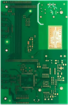
1. What is Double Layer PCB?
Double Layer PCB Definition
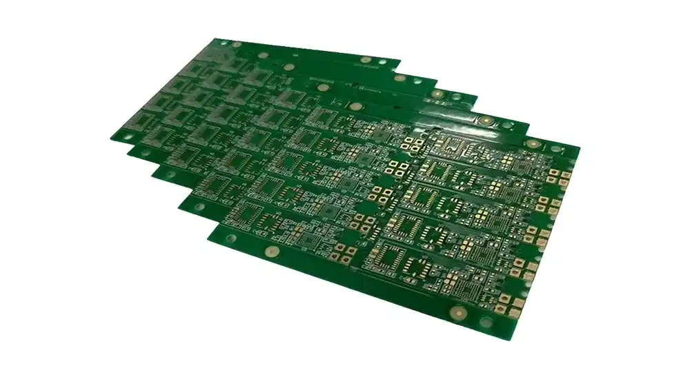
A double layer PCB, also known as a two-layer PCB or double-sided PCB, consists of two conductive copper layers separated by an insulating substrate material. Unlike single-layer boards that feature copper traces on only one side, double layer PCBs utilize both the top and bottom surfaces for circuit routing, significantly increasing design flexibility and component density.
Key Characteristics of Double Layer PCB
The fundamental structure includes a dielectric core material, typically FR4 fiberglass, with copper foil laminated to both surfaces. Electrical connections between the top and bottom layers are established through plated through-holes (PTHs), enabling complex circuit designs within a compact footprint.
Distinction from Other PCB Types
Double layer PCBs occupy the middle ground between simple single-layer boards and complex multilayer constructions. They offer substantially more routing capability than single-layer designs while remaining more cost-effective than multilayer alternatives for many applications.
2. Double Layer PCB Design
Design Requirements and Considerations
Double layer PCB design requires careful planning to optimize the use of both copper layers while maintaining signal integrity and electromagnetic compatibility. Engineers must consider trace routing strategies, component placement, and layer assignment to achieve optimal performance.
Critical Design Factors
1. Signal Routing Strategy: Designers typically assign power and ground connections to one layer while dedicating the opposite layer to signal traces. This approach minimizes interference and simplifies troubleshooting.
2. Via Placement and Management: Strategic via placement connects the two layers while minimizing signal degradation. Proper via stitching techniques ensure adequate current return paths and maintain signal integrity.
3. Component Density Optimization: The dual-sided nature allows for higher component density through strategic placement of components on both surfaces, reducing overall board size requirements.
Design Rule Considerations
Minimum trace width, spacing requirements, and via sizing must align with manufacturing capabilities and electrical requirements. Proper impedance control becomes increasingly important as signal frequencies increase.
3. Double Layer PCB Stackup
Standard Stackup Configuration
The typical double layer PCB stackup consists of four primary elements arranged in a symmetric structure. This configuration ensures mechanical stability while providing optimal electrical performance.
| Layer | Material | Typical Thickness | Function |
|---|---|---|---|
| Top Copper | Copper Foil | 0.5-2.0 oz (17-70 μm) | Signal/Power routing |
| Core Dielectric | FR4/Other | 0.4-3.2 mm | Insulation/Support |
| Bottom Copper | Copper Foil | 0.5-2.0 oz (17-70 μm) | Signal/Ground routing |
| Solder Mask | Polymer | 0.01-0.03 mm | Protection/Identification |
Electrical Performance Impact
The stackup configuration directly influences characteristic impedance, crosstalk, and electromagnetic interference. Proper dielectric selection and copper weight specification ensure optimal electrical performance for the intended application frequency range.
Mechanical Considerations
Symmetric copper distribution prevents board warpage during thermal cycling. The core material selection affects both mechanical strength and thermal expansion characteristics, critical factors for reliability in harsh environments.
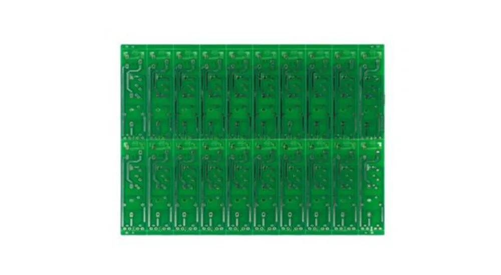
4. Double Layer PCB Manufacturing Process
Material Preparation and Setup
The manufacturing process begins with substrate preparation, where high-quality core materials undergo surface treatment to ensure optimal copper adhesion. Clean room environments maintain contamination-free processing throughout production.
Core Manufacturing Steps
1. Copper Cladding Process: Electrodeposited or rolled copper foil bonds to the prepared substrate through heat and pressure lamination. This process creates the foundational conductive layers for subsequent circuit formation.
2. Pattern Definition and Etching: Photolithographic processes transfer circuit patterns to the copper layers. Precise etching removes unwanted copper, leaving the desired circuit traces with accurate dimensions and spacing.
3. Drilling and Plating Operations: Computer-controlled drilling creates precise holes for component mounting and interlayer connections. Electrochemical plating deposits copper within the drilled holes, establishing electrical continuity between layers.
Quality Control and Testing
Automated optical inspection systems verify pattern accuracy and detect manufacturing defects. Electrical testing confirms connectivity and identifies potential reliability issues before final processing.
5. Double Layer PCB Assembly Process
Surface Mount Technology (SMT) Application
Modern double layer PCB assembly predominantly utilizes SMT components, which mount directly to copper pads on the board surface. This approach maximizes component density while enabling automated assembly processes.
Assembly Sequence and Methodology
1. Solder Paste Application: Precision stenciling deposits solder paste onto designated pads with controlled thickness and placement accuracy. Paste composition and rheology affect assembly quality and reliability.
2. Component Placement Operations: High-speed pick-and-place equipment positions components according to assembly drawings. Vision systems ensure accurate placement within specified tolerances.
3. Reflow Soldering Process: Controlled thermal profiles melt the solder paste, creating permanent electrical and mechanical connections. Multiple thermal zones accommodate components with varying thermal requirements.
Through-Hole Component Integration
When required, through-hole components integrate through selective wave soldering or hand soldering operations. Mixed-technology assemblies combine the benefits of both SMT and through-hole technologies.
Final Assembly Testing
In-circuit testing and functional verification ensure proper assembly quality. Automated test equipment validates electrical performance against design specifications.
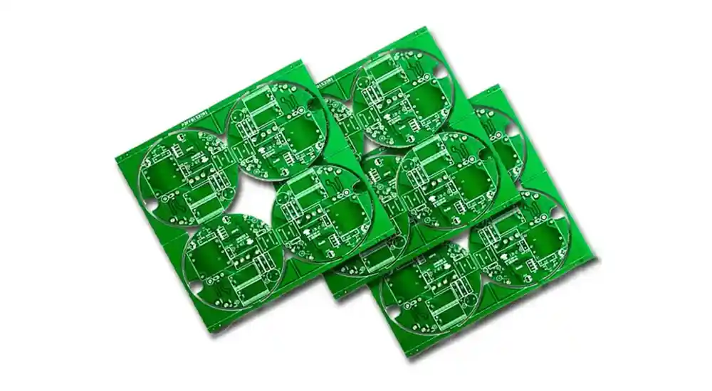
6. Double Layer PCB Materials
Core Substrate Materials
1. FR4 Fiberglass: The industry standard for most applications, FR4 offers excellent mechanical properties, thermal stability, and cost-effectiveness. Its glass transition temperature and dielectric properties suit the majority of electronic applications.
2. High-Frequency Materials: Applications requiring superior electrical performance utilize specialized substrates such as Rogers materials, which provide lower dielectric loss and stable electrical properties across wide frequency ranges.
3. Flexible Substrates: Polyimide-based materials enable flexible double layer PCBs for applications requiring mechanical flexibility or space constraints.
Copper Specifications
Copper weight selection depends on current-carrying requirements and thermal management needs. Standard weights range from 0.5 oz to 2.0 oz per square foot, with heavier copper available for high-power applications.
Surface Finish Options
| Surface Finish | Characteristics | Applications |
|---|---|---|
| HASL | Cost-effective, good solderability | General purpose |
| ENIG | Flat surface, wire bond compatible | Fine pitch components |
| OSP | Environmentally friendly, cost-effective | SMT assembly |
| Immersion Silver | Excellent electrical properties | High-frequency applications |
7. Double Layer PCB Cost
Primary Cost Factors
Double layer PCB pricing depends on multiple variables including board size, material selection, feature complexity, and production volume. Understanding these factors enables cost-effective design decisions.
Material Cost Components
Substrate material represents the largest cost component, with specialty materials commanding premium pricing. Copper weight and surface finish selection significantly impact material costs.
Manufacturing Complexity Impact
1. Feature Density: Finer trace widths and spacing require advanced manufacturing processes, increasing production costs. Standard design rules optimize the cost-performance balance.
2. Hole Count and Size: Drilling operations contribute significantly to manufacturing costs, particularly for small holes requiring specialized tooling.
3. Surface Finish Requirements: Premium surface finishes increase material and processing costs but may be necessary for specific applications.
Volume Economics
Production volume dramatically affects unit costs through setup amortization and material purchasing efficiency. Higher volumes enable more cost-effective manufacturing approaches.
Related Post
Key Cost Factors in Double Layer PCB Manufacturing
8. Double Layer PCB Thickness
Standard Thickness Options
Double layer PCBs are available in various thickness configurations to meet specific application requirements. Standard thicknesses provide optimal cost-performance balance for most applications.
| Standard Thickness | Applications | Characteristics |
|---|---|---|
| 0.4 mm | Compact devices | Maximum miniaturization |
| 0.8 mm | Consumer electronics | Good flexibility |
| 1.6 mm | General purpose | Industry standard |
| 2.4 mm | Industrial applications | Enhanced durability |
| 3.2 mm | Power electronics | Maximum current capacity |
Application-Specific Selection
1. Portable Electronics: Thinner boards reduce device profile and weight, critical factors for mobile applications. Mechanical flexibility accommodates device assembly requirements.
2. Industrial Equipment: Thicker boards provide enhanced mechanical strength and improved thermal management for harsh operating environments.
3. High-Power Applications: Increased thickness supports heavier copper weights and larger components while providing superior heat dissipation.
Design Trade-offs
Thickness selection involves balancing mechanical requirements, electrical performance, and cost considerations. Thinner boards may require additional mechanical support, while thicker boards increase material costs.
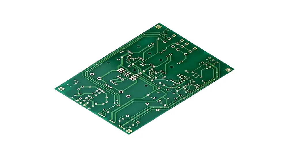
9. Types of Double Layer PCB
Standard FR4 Double Layer PCB
The most common configuration utilizes standard FR4 substrate with conventional copper weights. This approach provides excellent cost-effectiveness for general-purpose applications including consumer electronics and industrial controls.
High-Frequency Double Layer PCB
Specialized substrate materials optimize electrical performance for radio frequency and microwave applications. These boards feature controlled dielectric properties and low-loss materials essential for signal integrity.
Flexible Double Layer PCB
Polyimide-based flexible substrates enable dynamic flexing and space-constrained installations. These boards combine the routing advantages of double-layer construction with mechanical flexibility.
Heavy Copper Double Layer PCB
Enhanced copper weights support high-current applications and improved thermal management. These boards feature copper weights exceeding 2 oz per square foot, enabling power electronics and automotive applications.
Metal Core Double Layer PCB
Aluminum or copper core substrates provide superior thermal conductivity for LED lighting and power management applications. The metal core efficiently transfers heat away from temperature-sensitive components.
Related Post
Types of Double Layer PCB | Comprehensive Guide
10. Double Layer PCB Advantages and Disadvantages
Primary Advantages
1. Enhanced Circuit Density: Double layer construction enables significantly higher component density compared to single-layer alternatives. This capability reduces overall system size and weight while maintaining functionality.
2. Design Flexibility: The ability to route signals on both surfaces provides greater design freedom and simplified layout optimization. Complex circuits become feasible within compact footprints.
3. Cost-Effectiveness: Double layer PCBs offer an optimal balance between functionality and cost, providing enhanced capabilities without the expense of multilayer construction.
4. Improved Signal Integrity: Dedicated ground planes and controlled signal routing enhance electrical performance and reduce electromagnetic interference.
Potential Limitations
1. Complexity Constraints: While more capable than single-layer boards, double layer PCBs may not accommodate extremely complex circuits requiring multiple signal layers.
2. Via Dependency: Interlayer connections require vias, which consume board space and may introduce signal discontinuities in high-frequency applications.
3. Manufacturing Requirements: Double layer boards require more sophisticated manufacturing processes compared to single-layer alternatives, potentially affecting lead times and costs.
Performance Trade-offs
Design engineers must evaluate application requirements against double layer PCB capabilities to determine optimal board configuration. Many applications benefit significantly from the enhanced routing capability despite potential limitations.
11. Double Layer PCB Applications
Consumer Electronics Sector
Double layer PCBs form the foundation of countless consumer devices including smartphones, tablets, and home appliances. The enhanced routing capability enables compact designs with sophisticated functionality.
Automotive Electronics
Modern vehicles incorporate numerous double layer PCBs in engine management systems, infotainment platforms, and safety applications. The robust construction withstands automotive environmental requirements while providing reliable operation.
Industrial Control Systems
Manufacturing equipment and process control systems utilize double layer PCBs for sensor interfaces, motor controls, and communication modules. The enhanced signal integrity supports precise control and monitoring functions.
Medical Device Applications
Portable medical instruments and monitoring equipment benefit from the compact design possibilities of double layer construction. Strict regulatory requirements drive quality and reliability standards in this sector.
Telecommunications Infrastructure
Network equipment and communication devices employ double layer PCBs for signal processing and interface functions. High-speed digital signals require careful design attention to maintain signal integrity.
12. Single Layer PCB vs Double Layer PCB
Design Capability Comparison
Single layer PCBs limit circuit routing to one surface, constraining component density and trace routing options. Double layer boards effectively double the available routing area while enabling more sophisticated ground and power distribution strategies.
Cost Analysis
While double layer PCBs require higher initial investment than single-layer alternatives, the enhanced functionality often justifies the additional cost. Volume production reduces the cost differential significantly.
Manufacturing Complexity
Single layer boards utilize simpler manufacturing processes with fewer steps and quality control requirements. Double layer construction requires additional processes including plated through-hole formation and multilayer registration.
Application Suitability
1. Single Layer Applications: Simple circuits with minimal component counts and straightforward signal routing benefit from single layer construction. Cost-sensitive applications may prioritize simplicity over enhanced capability.
2. Double Layer Applications: Complex circuits requiring high component density, sophisticated signal routing, or enhanced electrical performance necessitate double layer construction.
Performance Characteristics
Double layer boards provide superior electromagnetic compatibility through dedicated ground planes and controlled signal routing. Single layer boards may require careful design attention to achieve adequate performance in electrically noisy environments.
13. Multilayer PCB vs Double Layer PCB
Design Complexity
Multilayer PCBs feature multiple layers of conductive copper separated by insulating materials, allowing for even more complex circuit designs compared to double layer PCBs. This additional complexity enables highly dense routing and greater flexibility in circuit layouts, while double layer PCBs provide a simpler, more cost-effective solution for less complex designs.
Cost Comparison
Multilayer PCBs are typically more expensive to produce than double layer PCBs due to the additional layers, materials, and more complex manufacturing processes involved. Double layer PCBs, on the other hand, offer a more budget-friendly option while still delivering enhanced routing capabilities compared to single-layer boards.
Manufacturing Process
While double layer PCBs are relatively straightforward to manufacture, multilayer PCBs require more intricate processes such as layer stacking, alignment, and interlayer bonding. The increased manufacturing steps for multilayer boards result in longer lead times and higher costs, which may not be justified for simpler applications.
Signal Integrity and Performance
Multilayer PCBs provide superior signal integrity due to better control of electromagnetic interference (EMI), higher component density, and more efficient power and ground planes. Double layer PCBs, though providing good signal integrity, may not match the performance of multilayer PCBs in high-frequency or high-performance applications.
Application Suitability
1. Multilayer PCB Applications: Complex devices requiring high-speed, high-frequency circuits such as telecommunications equipment, advanced computing systems, and medical devices benefit from multilayer designs.
2. Double Layer PCB Applications: Ideal for consumer electronics, automotive systems, and industrial controls, double layer PCBs offer an effective solution for less complex applications while still supporting higher component densities compared to single-layer boards.
Thermal Management
Multilayer PCBs are better equipped for thermal management due to the increased number of layers that can distribute heat more effectively across the board. Double layer PCBs may face challenges in thermal dissipation for power-intensive applications, but they can still perform adequately for most general-purpose uses.
Partner with Haoyue Electronics for Your Double Layer PCB Needs
Understanding double layer PCB technology is crucial for successful electronic product development, but partnering with an experienced manufacturer ensures optimal results. Haoyue Electronics combines advanced manufacturing capabilities with comprehensive engineering support to deliver high-quality double layer PCBs that meet your specific requirements.
Our state-of-the-art facilities utilize the latest manufacturing technologies and quality control systems to produce double layer PCBs with exceptional reliability and performance. From prototype development through high-volume production, our experienced team provides technical guidance and manufacturing expertise to optimize your designs for both performance and cost-effectiveness.
Whether your application demands standard FR4 construction or specialized materials for high-frequency performance, Haoyue Electronics has the capabilities and experience to deliver superior results. Our comprehensive services include design review, manufacturing optimization, and complete PCB assembly services, providing a single-source solution for your electronic manufacturing needs.
Contact Haoyue Electronics today to discuss your double layer PCB requirements and discover how our expertise can accelerate your product development while ensuring the highest quality standards.

