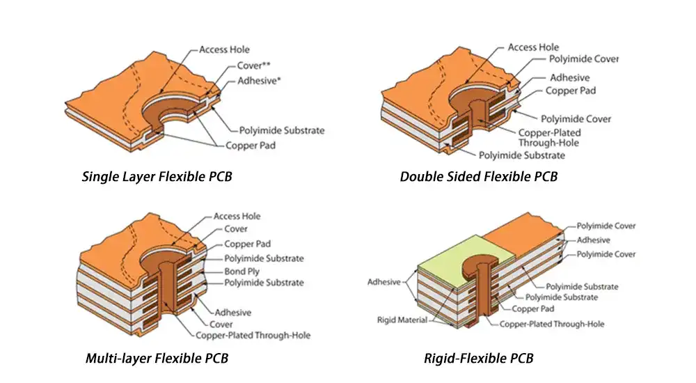
Flexible printed circuit boards represent a revolutionary advancement in electronic design, offering unparalleled versatility for applications requiring bendable, lightweight, and space-efficient solutions. As electronic devices continue to evolve toward more compact and sophisticated designs, understanding the distinct characteristics and applications of different flexible PCB types becomes crucial for engineers and designers.
This comprehensive guide examines the four primary categories of flexible PCB technology, their unique features, manufacturing considerations, and optimal use cases.
Check out our in-depth article on The Ultimate Guide to Flexible PCBs, or explore our Complete Flexible PCB Design Guide to assist you in crafting your next flexible PCB design.
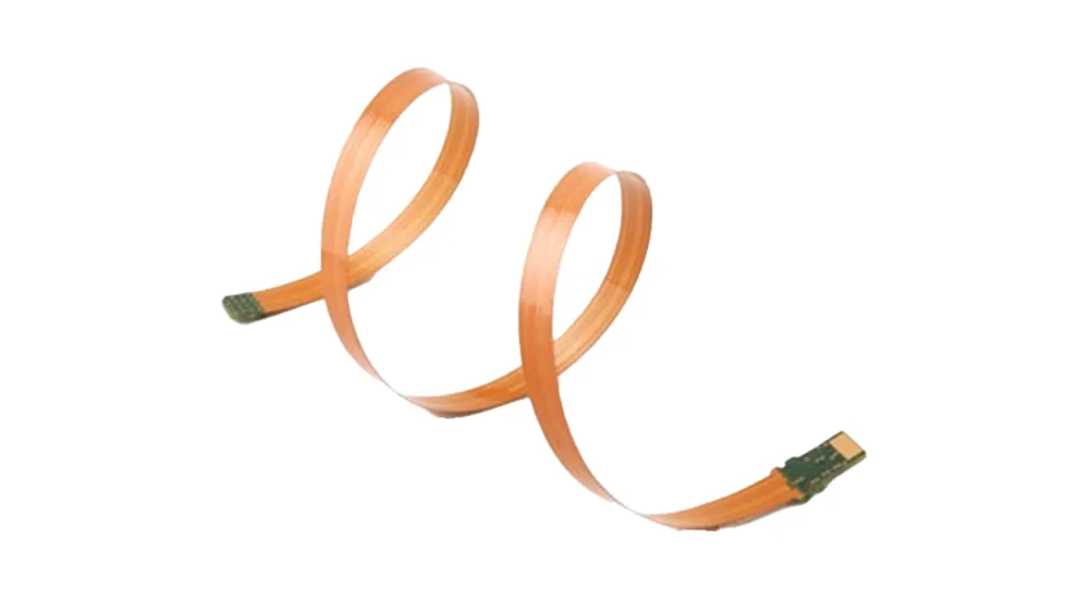
Single Layer Flexible PCB: Foundation of Flexible Electronics
Single layer flexible PCB technology represents the most fundamental and widely adopted form of flexible circuit board design. These circuits consist of a single conductive copper layer laminated between protective polyimide or polyester substrates, creating a basic yet highly effective flexible interconnect solution.
Construction and Materials
The construction of single layer flexible PCBs involves several critical components that determine their performance characteristics:
- Base substrate: Typically polyimide film ranging from 12 to 125 microns in thickness
- Copper conductor: Usually electrodeposited copper varying from 0.5 to 2 ounces per square foot
- Adhesive layer: Acrylic or epoxy-based bonding agents for substrate adhesion
- Cover layer: Protective polyimide or solder mask coating
Applications and Advantages
Single layer flexible PCBs excel in applications requiring simple point-to-point connections with minimal space constraints. These circuits are particularly effective in consumer electronics, automotive sensors, medical devices, and industrial equipment where basic connectivity and flexibility are primary requirements.
The manufacturing simplicity of single layer designs translates to cost-effective production, making them ideal for high-volume applications. Their reduced thickness and weight characteristics provide significant advantages in portable devices and space-constrained environments.
Design Considerations
When designing single layer flexible PCBs, engineers must carefully consider trace width, spacing, and bend radius requirements. The absence of multiple layers necessitates strategic trace routing to avoid crossovers while maintaining signal integrity and mechanical reliability.
Related Reading
· Single Layer PCB Types
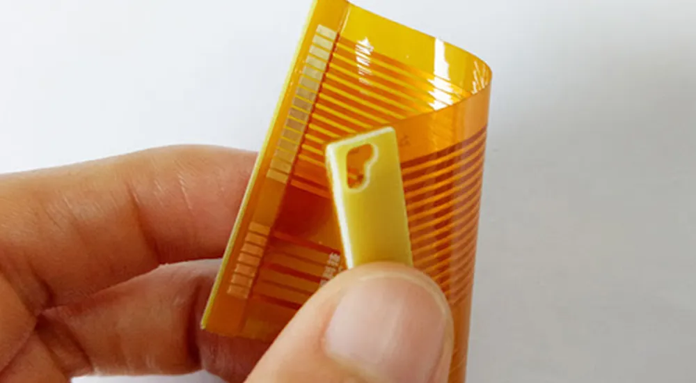
Double Sided Flexible PCB: Enhanced Connectivity Solutions
Double sided flexible PCB technology expands design possibilities by incorporating conductive copper layers on both sides of the flexible substrate. This configuration enables more complex circuit designs while maintaining the inherent flexibility advantages of single layer constructions.
Technical Architecture
Double sided flexible PCBs feature copper conductors on both the top and bottom surfaces of the polyimide substrate, connected through plated through-holes or vias. This dual-layer approach significantly increases routing density and enables more sophisticated circuit topologies.
Manufacturing Process Considerations
The production of double sided flexible PCBs requires additional processing steps compared to single layer variants:
- Sequential copper deposition on both substrate surfaces
- Through-hole drilling and plating operations
- Precise registration alignment between layers
- Enhanced quality control procedures for via reliability
Performance Benefits
Double sided flexible PCB designs offer substantial advantages for applications requiring increased circuit density without compromising flexibility. The ability to route traces on both surfaces enables more efficient use of available space while maintaining the mechanical properties essential for dynamic flexing applications.
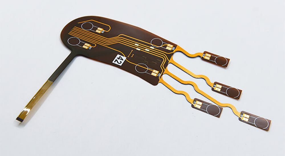
Multi-Layer Flexible PCB: Advanced Circuit Integration
Multi-layer flexible PCB technology represents the pinnacle of flexible circuit design, incorporating three or more conductive layers within a single flexible assembly. These sophisticated circuits enable complex signal routing, controlled impedance characteristics, and enhanced electromagnetic interference shielding capabilities.
Layer Stack-up Configuration
Multi-layer flexible PCBs typically incorporate alternating layers of copper conductors and polyimide dielectric materials, creating a laminated structure that maintains flexibility while providing advanced electrical performance. Common configurations include four, six, and eight-layer designs, with specialized applications requiring even higher layer counts.
Advanced Design Features
The multiple layer architecture enables several advanced design features that distinguish these circuits from simpler flexible PCB types:
- Controlled impedance traces: Precise dielectric thickness control for high-frequency signal integrity
- Shielding layers: Dedicated ground and power planes for electromagnetic compatibility
- Differential pair routing: Optimized trace geometry for high-speed digital signals
- Thermal management: Strategic copper distribution for heat dissipation
Manufacturing Complexity and Quality Control
Multi-layer flexible PCB production requires sophisticated manufacturing processes and stringent quality control measures. The lamination process must achieve precise layer alignment while maintaining uniform dielectric thickness across the entire circuit area. Advanced testing procedures, including impedance measurement and cross-sectional analysis, ensure compliance with demanding performance specifications.
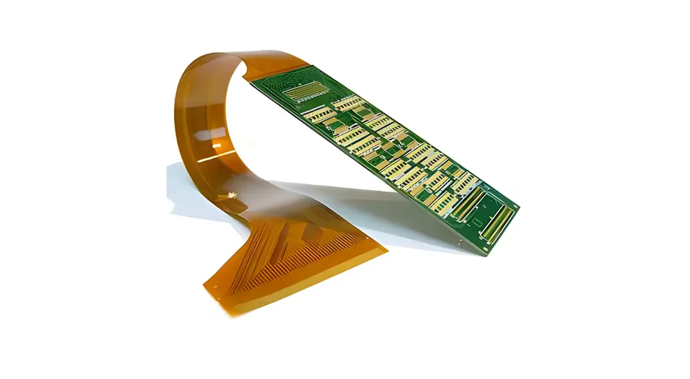
Rigid-Flex PCB: Hybrid Technology Solutions
Rigid-flex PCB technology combines the benefits of traditional rigid printed circuit boards with flexible interconnect sections, creating hybrid assemblies that optimize both mechanical stability and design flexibility. This innovative approach eliminates the need for separate connectors and cables while providing robust mounting platforms for components.
Architectural Design Principles
Rigid-flex PCBs feature distinct rigid and flexible sections within a single integrated assembly. The rigid portions provide stable mounting platforms for components and connectors, while the flexible sections enable three-dimensional routing and dynamic movement capabilities.
Construction Methodology
The manufacturing process for rigid-flex PCBs involves several specialized techniques:
- Selective lamination: Rigid sections receive additional substrate layers for increased thickness and stability
- Transition zone engineering: Gradual thickness changes between rigid and flexible areas minimize stress concentrations
- Component placement optimization: Strategic positioning of components within rigid zones for maximum reliability
Application Advantages
Rigid-flex PCB technology offers compelling advantages for applications requiring both structural integrity and flexible interconnection. Aerospace systems, medical devices, and high-reliability industrial equipment benefit from the reduced assembly complexity and enhanced reliability characteristics of rigid-flex designs.
Comparative Analysis and Selection Guidelines
Selecting the appropriate flexible PCB type requires careful consideration of multiple factors including electrical requirements, mechanical constraints, manufacturing volume, and cost targets. The following comparison framework assists in making informed technology decisions:
| PCB Type | Layer Count | Complexity | Cost | Typical Applications |
|---|---|---|---|---|
| Single Layer | 1 | Low | Lowest | Simple interconnects, sensors |
| Double Sided | 2 | Medium | Medium | Enhanced connectivity, displays |
| Multi-Layer | 3+ | High | Higher | High-speed signals, complex circuits |
| Rigid-Flex | Variable | Highest | Highest | 3D assemblies, space-critical designs |
Performance Considerations
When evaluating flexible PCB options, engineers should assess several critical performance parameters:
- Signal integrity requirements: High-frequency applications may necessitate multi-layer designs with controlled impedance characteristics
- Mechanical stress factors: Dynamic flexing applications require careful material selection and bend radius optimization
- Environmental conditions: Temperature extremes, chemical exposure, and humidity levels influence material choices
- Assembly complexity: Component density and interconnection requirements impact layer count decisions
Future Trends and Technology Evolution
The flexible PCB industry continues to evolve with advancing materials science, manufacturing techniques, and application requirements. Emerging trends include ultra-thin substrate materials, embedded component technology, and advanced shielding solutions for high-frequency applications.
Ready to bring your flexible PCB designs to life? Haoyue Electronics combines decades of manufacturing expertise with cutting-edge production capabilities to deliver superior flexible PCB solutions across all technology types. Our experienced engineering team provides comprehensive design support, from initial concept through full-scale production, ensuring your flexible circuit requirements are met with precision and reliability.
Whether you need cost-effective single layer solutions or sophisticated multi-layer rigid-flex assemblies, our ISO-certified facilities and rigorous quality processes guarantee consistent results that exceed industry standards. Contact Haoyue Electronics today to discuss your flexible PCB requirements and discover how our technical expertise can accelerate your next innovative project.

