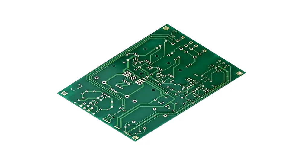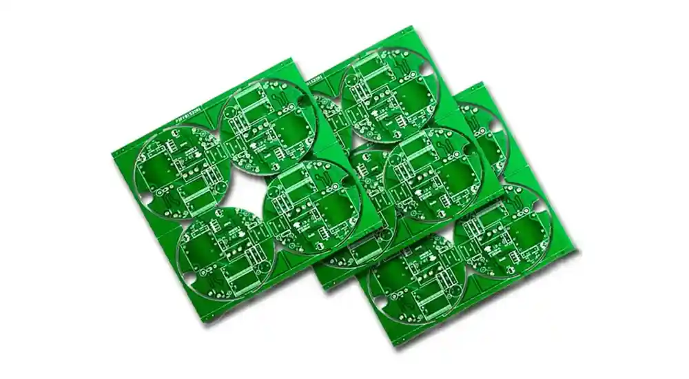
The primary classification of double layer PCB types encompasses substrate-based categorization, application-specific configurations, and structural variations. According to the nature of the PCB substrate, PCB can generally be divided into Rigid PCB, Flexible PCB (FPC), and Rigid-flex PCB, with each category supporting double layer implementations. Additionally, material-based classifications include double-sided high-frequency PCBs, double-sided metal core PCBs, double-sided flexible PCBs, double-sided ceramic PCBs, and hybrid configurations that combine multiple technologies.
1. FR-4 Based Double Layer PCBs
Standard FR-4 Double Layer Construction
Double-sided PCBs (also known as Double-Sided Plated Through or DSPT) are the foundation for more advanced technology applications. FR-4 is the most commonly used substrate material for double layer PCB manufacturing due to its exceptional balance of electrical properties, mechanical strength, and cost-effectiveness.
FR-4 double layer PCBs feature copper conductors laminated on both sides of a flame-retardant fiberglass substrate. FR-4 is widely used across various industries to manufacture single-sided, double-sided, and multi-layered boards. The dielectric constant typically ranges from 4.2 to 4.8, making these boards suitable for applications operating at frequencies up to several hundred megahertz.
High-Frequency FR-4 Variants
Advanced FR-4 formulations incorporate modified resin systems and glass weave patterns to improve high-frequency performance. These variants maintain the manufacturing advantages of standard FR-4 while offering reduced dielectric loss and more stable electrical characteristics across varying temperatures.
2. Metal Core Double Layer PCBs
Aluminum-Based Double Layer PCBs
Double-sided metal core PCBs include both double-sided aluminum PCBs and double-sided copper core PCBs. These are primarily used in LED lighting applications that require efficient thermal dissipation. Aluminum-based double layer PCBs excel in thermal management, where effective heat dissipation is critical for maintaining component reliability and performance.
The construction typically features copper circuits on both sides of an aluminum core, with dielectric layers providing electrical isolation while maintaining thermal conductivity. Common applications include high-power LED arrays, automotive lighting systems, and power electronics, where thermal performance directly affects the operational lifetime of components.
Copper Core Double Layer PCBs
Copper core substrates offer superior thermal conductivity compared to aluminum, making them ideal for extreme thermal management needs. Double-sided copper core PCBs are more costly than single-sided versions, but the enhanced thermal performance justifies the investment in demanding applications such as high-power RF amplifiers and industrial motor drives.
3. Flexible Double Layer PCBs
Polyimide-Based Flexible PCBs
The base material for double-sided flexible PCBs and rigid-flex PCBs is polyimide (PI) or polyethylene terephthalate (PET). PI and PET are used as the substrate and dielectric layers in double-sided flexible PCBs. Polyimide-based flexible double layer PCBs offer exceptional reliability in dynamic applications that require repeated flexing cycles.
These boards support complex three-dimensional packaging requirements while maintaining excellent electrical performance. Copper foil selection is crucial, with rolled annealed (RA) copper providing superior flexibility compared to electrodeposited (ED) copper.
PET-Based Flexible Double Layer PCBs
Polyethylene terephthalate (PET) substrates offer cost benefits for applications with less demanding flexibility requirements. While PET has lower temperature tolerance compared to polyimide, PET-based double layer flexible PCBs are ideal for consumer electronics and disposable medical devices, where cost optimization is critical.
4. High-Frequency Double Layer PCBs
PTFE-Based High-Frequency PCBs
The key to double-sided high-frequency PCBs is the laminate. PTFE (polytetrafluoroethylene) laminates should have minimal thermal expansion and contraction. PTFE substrates offer superior performance in microwave and millimeter-wave applications due to their low dielectric loss and excellent frequency stability.
Rogers RO3000 and RO4000 series materials are popular choices for double layer high-frequency implementations. These materials are favored for their ease of machining and low dielectric losses at microwave frequencies, making them ideal for flexible circuit applications.
Ceramic-Filled High-Frequency PCBs
Ceramic-filled hydrocarbon substrates provide intermediate performance between FR-4 and PTFE materials while offering improved cost-effectiveness for moderate high-frequency applications. These materials typically exhibit dielectric constants in the 3.0 to 3.5 range, with loss tangents below 0.004, making them suitable for moderate-frequency applications that require cost efficiency.
5. Ceramic Double Layer PCBs
Aluminum Nitride Double Layer PCBs
Double-sided ceramic PCBs include aluminum nitride (AlN) and alumina PCBs. Both AlN and alumina offer excellent thermal conductivity, stable chemical properties, and low thermal expansion. Aluminum nitride substrates demonstrate exceptional thermal conductivity exceeding 180 W/mK, making them ideal for high-power semiconductor applications.
The fabrication of ceramic PCBs requires specialized techniques due to their brittle nature. The stack-up of a two-layer double-sided AlN PCB typically follows this structure: copper > AlN substrate > copper, or copper > dielectric layer > AlN substrate > dielectric layer > copper.
Alumina Double Layer PCBs
Alumina substrates offer excellent electrical insulation properties combined with good thermal performance, all at a lower cost compared to aluminum nitride. These boards are particularly effective in RF power applications, hybrid circuits, and high-temperature electronics, where dimensional stability is critical.

6. CEM-Series Double Layer PCBs
CEM-1 Double Layer PCBs
CEM-1 is made with a phenolic resin binder, providing good mechanical strength and rigidity. However, its limitations in hole metallization restrict its use primarily to single-sided applications. Specialized manufacturing techniques, however, enable the creation of double layer CEM-1 PCBs for cost-sensitive applications that require moderate performance.
CEM-3 Double Layer PCBs
CEM-3 is commonly used in double-sided PCBs with plated holes and typically costs about $1 to $2 less per square meter than FR-4. CEM-3 substrates combine glass cloth reinforcement with composite materials, offering enhanced mechanical properties compared to paper-based alternatives while maintaining cost benefits over FR-4.
7. Rigid-Flex Double Layer PCBs
Hybrid Construction PCBs
Rigid-Flex PCBs combine the characteristics of rigid and flexible circuit boards, meeting the process requirements of both. Double layer rigid-flex constructions allow for complex three-dimensional assemblies while eliminating the need for traditional connectors.
The flexible sections typically use polyimide substrates with rolled annealed copper, while the rigid sections employ FR-4 or other conventional materials. This combination provides mechanical stability in mounting areas while accommodating dynamic flexing in interconnect regions.
8. Specialized Double Layer PCB Types
Thick Copper Double Layer PCBs
Heavy copper double layer PCBs incorporate copper weights exceeding 2 oz/ft² (70 μm) to support high-current applications. These constructions require specialized etching and plating processes to ensure dimensional accuracy while achieving the necessary conductor thickness.
Applications include power distribution systems, automotive electronics, and industrial controls, where current-carrying capacity takes precedence over density considerations. The thermal mass of thick copper conductors also provides enhanced heat dissipation capabilities.
HDI Double Layer PCBs
High Density Interconnect (HDI) double layer PCBs use microvias and fine-line lithography to achieve component densities comparable to multilayer boards. HDI technology enables a denser design, resulting in smaller PCBs with more traces and components in a given area.
Blind and buried via technologies facilitate complex routing within the double layer constraint while maintaining the compact form factors necessary for portable electronics and miniaturized systems.

Selection Criteria and Applications
Performance Requirements Analysis
Selecting the appropriate double layer PCB type requires a comprehensive evaluation of electrical, mechanical, and thermal requirements. Signal integrity, which ensures the quality of waveforms and reliable information transmission, is critical for high-speed applications, making careful substrate selection and stackup design essential.
Key evaluation parameters include operating frequency range, current-carrying requirements, thermal dissipation needs, environmental conditions, and cost constraints. Each parameter influences material selection and construction techniques, ultimately determining the optimal double layer PCB configuration.
Application-Specific Considerations
Consumer electronics typically use FR-4 double layer PCBs due to their cost-effectiveness and adequate performance for moderate-frequency applications. In medical devices, precision and reliability are critical, making double layer PCBs the preferred choice, often requiring enhanced materials for improved reliability.
Automotive applications demand materials capable of withstanding extended temperature cycling and vibration exposure, often requiring CEM-3 or specialized FR-4 variants. Industrial systems may require metal core substrates for thermal management or ceramic materials for resistance to harsh environments.
Manufacturing Considerations
Process Complexity and Cost Implications
Double-sided PCBs are the most commonly used and preferred type due to their balance between the complexity of multilayer PCBs and the simplicity of single-layer PCBs. Manufacturing double layer PCBs involves additional steps compared to single-sided alternatives, including through-hole plating and dual-sided imaging.
Manufacturing double-sided PCBs requires drilling through holes and electroplating them with copper. These additional steps impact production timelines and costs but enable enhanced functionality and greater routing density.
Quality Control and Testing
Double layer PCB manufacturing requires comprehensive testing to ensure interlayer connectivity and electrical performance. Automated optical inspection systems check conductor integrity on both sides, while electrical testing validates through-hole plating quality and impedance characteristics.
Conclusion
Double layer PCB technology encompasses a wide range of material systems and construction techniques, each tailored to meet specific application needs. From cost-effective FR-4 solutions for consumer electronics to high-performance ceramic substrates for demanding aerospace applications, understanding the available options enables more informed design decisions.
The selection process involves balancing performance requirements with cost constraints, while also considering manufacturing complexity and long-term reliability. As electronic systems continue to evolve toward higher frequencies, increased power densities, and miniaturized form factors, double layer PCB technology adapts to meet these challenges through innovative materials and construction techniques.
Partner with Haoyue Electronics for Expert Double Layer PCB Solutions
At Haoyue Electronics, we understand that selecting the right double layer PCB type is crucial for the success of your project. Our experienced engineering team specializes in manufacturing precision double layer PCBs across all major substrate types, from standard FR-4 to advanced ceramic and high-frequency materials.
With over a decade of experience in PCB manufacturing and assembly, we provide comprehensive support from initial design consultation through final testing and delivery. Our state-of-the-art facilities ensure consistent quality and rapid turnaround times for both prototype and production volumes.
Whether you require aluminum core PCBs for LED applications, high-frequency PTFE substrates for RF designs, or flexible polyimide constructions for dynamic environments, Haoyue Electronics delivers tailored solutions that meet your exact specifications. Contact our technical team today to discuss your double layer PCB requirements and discover how our expertise can accelerate your project timeline while ensuring optimal performance and reliability.
FAQ
1. What is the main difference between single layer and double layer PCBs?
The key difference is the number of copper layers. Single layer PCBs have copper traces on one side, limiting routing density and component placement. Double layer PCBs have copper on both sides, connected by vias, doubling the available routing area. This allows for more complex designs, better signal integrity, and the ability to mount components on both sides. Double layer PCBs are ideal for higher component density and electrical performance at a lower cost than multilayer alternatives.
2. How do I choose the right substrate material for my double layer PCB application?
Choose substrate materials based on electrical, thermal, and mechanical needs. FR-4 is suitable for general-purpose applications under 1 GHz. For high-frequency use, PTFE-based materials like Rogers RO4000 reduce signal loss. For thermal management, aluminum or copper core substrates offer better heat dissipation. Flexible applications require polyimide, while harsh environments may need ceramic substrates for superior durability.
3. What are the cost implications of different double layer PCB types?
FR-4 double layer PCBs are the most cost-effective, costing 15-25% more than single-sided boards. CEM-3 offers a 10-20% cost saving compared to FR-4. High-frequency PTFE substrates cost 300-500% more than FR-4, while metal core substrates are 200-400% pricier. Flexible polyimide substrates are 150-300% more expensive. Production volume significantly affects unit costs, with higher volumes offering better pricing.
4. Can double layer PCBs handle high-frequency applications effectively?
Yes, double layer PCBs handle high-frequency applications well when designed with appropriate substrates like PTFE (e.g., Rogers RO3000). Key design considerations include controlled impedance, continuous reference planes, and minimized parasitic effects. Advanced HDI constructions can achieve near-multilayer performance while maintaining cost advantages. These PCBs are used in applications such as cellular infrastructure, automotive radar, and satellite communications, supporting frequencies over 10 GHz.
5. What manufacturing capabilities should I look for in a double layer PCB supplier?
Look for suppliers with precision drilling, advanced plating systems, and fine-line imaging capabilities. Quality control should include automated optical inspection and electrical testing for interlayer connectivity. Expertise in handling materials like PTFE, ceramic, and flexible substrates is essential. Choose suppliers with design-for-manufacturability services, prototype capabilities, and certifications like ISO 9001 and IATF 16949 for automotive. Technical support in impedance modeling and thermal analysis adds value in the development process.

