Understanding PCB Layer Configurations
Single Layer PCB Architecture
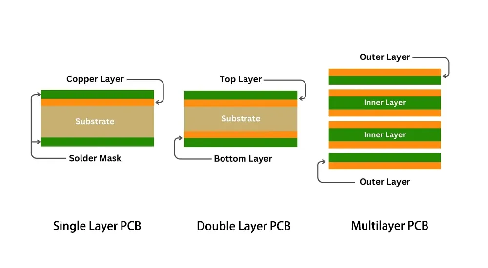
A single layer PCB, also known as a single-sided PCB, features conductive traces exclusively on one side of the substrate material. This configuration represents the most basic form of printed circuit board construction, where electronic components are mounted on the component side while the copper traces and pads reside on the opposite surface. The substrate typically consists of FR-4 fiberglass or phenolic resin materials that provide mechanical support and electrical insulation.
The manufacturing process for single layer PCBs involves applying copper foil to one side of the substrate, followed by photolithographic etching to create the desired circuit pattern. Component mounting occurs through holes drilled from the component side to the copper layer, where solder connections establish electrical continuity. This straightforward construction method results in lower manufacturing costs and reduced production complexity compared to more advanced PCB configurations.
Double Layer PCB Construction
Double layer PCB designs incorporate conductive traces on both sides of the substrate material, connected through plated through-holes (PTHs) or vias. This configuration significantly increases routing density and provides enhanced design flexibility compared to single layer alternatives. The top layer typically accommodates surface-mount components, while the bottom layer serves for additional routing and through-hole component connections.
The manufacturing process for double layer PCBs requires precise alignment between the top and bottom copper layers during lamination. Plated through-holes create electrical connections between layers, enabling complex circuit designs within a compact form factor. This bi-directional routing capability allows designers to implement more sophisticated electronic circuits while maintaining reasonable manufacturing costs.
Multilayer PCB Technology
Multilayer PCB constructions feature three or more conductive layers separated by insulating dielectric materials. These advanced configurations enable high-density circuit designs essential for modern electronic applications. Common multilayer configurations include four-layer, six-layer, eight-layer, and more complex arrangements depending on application requirements.
The manufacturing process involves sequential lamination of alternating copper and dielectric layers under controlled temperature and pressure conditions. Buried vias connect internal layers, while through-holes provide connections across the entire stack-up. This sophisticated construction enables complex signal routing, dedicated power and ground planes, and enhanced electromagnetic interference (EMI) shielding capabilities.

Performance Characteristics and Electrical Properties
Signal Integrity Considerations
Single layer PCBs exhibit limited signal integrity performance due to the absence of dedicated ground planes and restricted routing options. Signal traces must share common return paths, potentially creating ground loops and noise interference. The single-sided configuration also limits the implementation of controlled impedance traces, which are essential for high-frequency applications.
Double layer PCBs provide significant signal integrity improvements through the implementation of ground planes or dedicated return paths. The availability of both top and bottom copper layers enables better power distribution and reduced electromagnetic interference. However, maintaining consistent impedance control across layer transitions requires careful design consideration.
Multilayer PCBs offer superior signal integrity performance through dedicated power and ground planes that provide stable reference voltages and minimize electromagnetic interference. The ability to implement differential pairs, controlled impedance traces, and strategic layer stacking optimizes high-frequency signal transmission. Advanced multilayer designs can achieve impedance tolerances within ±10% across the entire frequency spectrum.
Power Distribution and Thermal Management
Single layer PCBs rely on trace width and copper thickness to handle current requirements, often resulting in wider traces that consume valuable board real estate. Thermal dissipation depends primarily on the copper area and substrate thermal conductivity, limiting power handling capabilities.
Double layer PCBs enable improved power distribution through dedicated power and ground routing on separate layers. The increased copper area enhances current-carrying capacity and thermal dissipation compared to single layer alternatives. Strategic placement of power traces on both layers distributes heat more effectively across the board surface.
Multilayer PCBs excel in power distribution and thermal management through dedicated power planes that provide low-impedance current paths and efficient heat spreading. The multiple copper layers create effective thermal conduction paths, while the increased board thickness accommodates higher power densities. Advanced thermal management techniques, including thermal vias and heat-spreading layers, further enhance power handling capabilities.

Manufacturing Complexity and Cost Analysis
Production Processes and Equipment Requirements
Single layer PCB manufacturing utilizes standard printed circuit board fabrication equipment with minimal process complexity. The single-sided etching process requires fewer chemical baths and shorter processing times compared to multilayer alternatives. Quality control procedures focus primarily on dimensional accuracy and copper adhesion, simplifying the inspection process.
Double layer PCB production introduces additional complexity through the requirement for precise layer alignment and plated through-hole processing. The manufacturing sequence involves sequential imaging, etching, and plating operations for both copper layers. Quality control must verify interlayer connectivity and registration accuracy, increasing inspection requirements.
Multilayer PCB manufacturing demands sophisticated equipment and precise process control throughout the fabrication sequence. The lamination process requires controlled temperature and pressure profiles to achieve proper bonding between layers. Sequential drilling and plating operations create complex interconnection structures that require advanced testing and verification procedures.
Cost Structure and Economic Considerations
| PCB Type | Material Cost | Manufacturing Cost | Tooling Requirements | Lead Time |
|---|---|---|---|---|
| Single Layer | Low | Minimal | Basic | 1-3 days |
| Double Layer | Medium | Moderate | Standard | 3-7 days |
| Multilayer | High | Complex | Advanced | 7-14 days |
Single layer PCBs represent the most cost-effective option for simple electronic applications, with material costs limited to substrate and single copper layer requirements. The streamlined manufacturing process minimizes labor costs and equipment utilization, resulting in competitive pricing for high-volume production.
Double layer PCBs incur moderate cost increases due to additional copper layers and plated through-hole processing. The enhanced functionality and routing density often justify the increased investment for applications requiring improved performance characteristics.
Multilayer PCBs command premium pricing due to complex manufacturing processes, specialized materials, and extended fabrication times. However, the superior performance characteristics and design flexibility often provide favorable cost-per-function ratios for advanced electronic applications.

Application-Specific Selection Criteria
Single Layer PCB Applications
Single layer PCBs excel in cost-sensitive applications where circuit complexity remains minimal and performance requirements are modest. Consumer electronics, simple LED lighting systems, and basic control circuits represent ideal applications for single layer designs. The straightforward manufacturing process enables rapid prototyping and high-volume production for price-competitive markets.
Radio frequency (RF) applications may benefit from single layer designs when ground plane requirements are minimal and circuit isolation is not critical. Simple amplifier circuits, basic filter networks, and low-frequency oscillators can achieve satisfactory performance with single layer implementations.
Double Layer PCB Applications
Double layer PCBs serve as optimal solutions for moderate complexity circuits requiring enhanced routing density and improved signal integrity. Microcontroller-based systems, power supply circuits, and digital communication interfaces benefit from the increased design flexibility and performance characteristics.
The availability of dedicated ground planes makes double layer PCBs suitable for mixed-signal applications where analog and digital circuits coexist. The improved power distribution capabilities support moderate power requirements while maintaining acceptable thermal performance.
Multilayer PCB Applications
Multilayer PCBs are essential for high-performance electronic systems requiring complex interconnections and superior signal integrity. Advanced microprocessor systems, high-speed digital interfaces, and precision analog circuits demand the sophisticated capabilities provided by multilayer designs.
Modern telecommunications equipment, aerospace electronics, and medical devices rely on multilayer PCBs to achieve the performance standards required for critical applications. The ability to implement controlled impedance traces, dedicated power planes, and advanced electromagnetic shielding makes multilayer designs indispensable for contemporary electronic systems.
Performance Comparison Summary
The selection between single layer PCB, double layer PCB, and multilayer PCB configurations depends on application requirements, performance specifications, and economic constraints. To facilitate informed decision-making, the following comparison table summarizes the key characteristics of each PCB type:
| Characteristic | Single Layer PCB | Double Layer PCB | Multilayer PCB |
|---|---|---|---|
| Complexity | Simple | Moderate | Complex |
| Cost | Low | Medium | High |
| Signal Integrity | Limited | Good | Excellent |
| Routing Density | Low | Medium | High |
| Power Distribution | Basic | Improved | Superior |
| EMI Shielding | Minimal | Moderate | Excellent |
| Thermal Management | Limited | Good | Superior |
| Manufacturing Time | Fast (1-3 days) | Standard (3-7 days) | Extended (7-14 days) |
| Ideal Applications | Simple circuits, LED lighting | Microcontrollers, power supplies | High-speed digital, RF systems |
| Maximum Frequency | Low-Medium | Medium-High | Very High |
Single layer designs provide cost-effective solutions for simple circuits with minimal performance requirements. Double layer configurations offer balanced performance and cost characteristics suitable for moderate complexity applications. Multilayer designs deliver superior performance capabilities essential for advanced electronic systems.
Understanding these fundamental differences enables informed decision-making throughout the product development process. The optimal PCB layer configuration balances technical requirements with manufacturing constraints to achieve successful electronic product implementation.
Partner with Haoyue Electronics for Your PCB Manufacturing Needs
At Haoyue Electronics, we provide high-quality PCB manufacturing across all layer types—from simple single layer boards to complex multilayer assemblies. Equipped with advanced fabrication technology, we can produce up to 32-layer PCBs with precise tolerances and excellent surface finishes.
Our ISO 9001:2015-certified process ensures rigorous quality control and reliable performance. We offer engineering support including DFM analysis, material selection, and process optimization to streamline your development.
With comprehensive testing capabilities and flexible production capacity—from prototypes to mass production—we deliver cost-effective solutions tailored to your technical needs. Whether for consumer electronics or aerospace, our experienced team is ready to support your project from design through manufacturing.
Contact us to explore how Haoyue Electronics can help optimize your next PCB project.

