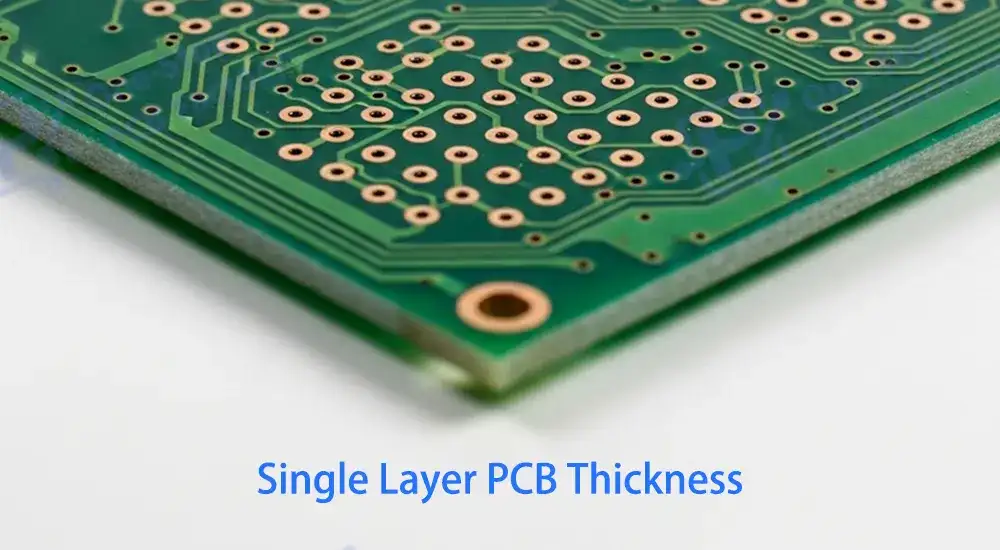
Single layer PCB thickness represents one of the most fundamental design parameters in electronic circuit manufacturing, directly influencing electrical performance, mechanical stability, and manufacturing feasibility. As electronic devices continue to miniaturize while demanding enhanced functionality, understanding the nuances of single layer PCB thickness becomes crucial for engineers, designers, and manufacturers seeking optimal circuit board solutions.
The thickness of a single layer printed circuit board encompasses the total substrate material depth, including the base dielectric material and copper traces. This seemingly simple parameter carries significant implications for signal integrity, thermal management, and overall system reliability, making it a critical consideration in the design and manufacturing process.
Understanding Single Layer PCB Thickness Specifications
Standard Thickness Ranges and Industry Guidelines
Single layer PCB thickness typically ranges from 0.4mm to 3.2mm, with specific applications driving the selection of optimal thickness values. The most commonly utilized thicknesses in commercial applications include:
| Thickness Range | Primary Applications | Key Characteristics |
|---|---|---|
| 0.4mm - 0.6mm | Ultra-thin consumer electronics, wearables | Maximum miniaturization, flexibility considerations |
| 0.8mm - 1.0mm | Standard consumer products, mobile devices | Balanced performance and manufacturability |
| 1.2mm - 1.6mm | Industrial applications, automotive electronics | Enhanced mechanical strength, thermal stability |
| 2.0mm - 3.2mm | High-power applications, specialized equipment | Superior heat dissipation, robust construction |
The selection of appropriate single layer PCB thickness depends on multiple engineering considerations, including the intended application environment, electrical requirements, and mechanical constraints. Standard thicknesses of 0.8mm, 1.2mm, and 1.6mm represent the most frequently specified options due to their optimal balance of performance characteristics and manufacturing efficiency.
Material Composition and Substrate Considerations
Single layer PCB thickness is primarily determined by the substrate material, typically FR-4 (Flame Retardant 4) fiberglass, which provides the structural foundation for the circuit board. The substrate thickness directly correlates with the board’s mechanical properties, including flexural strength, dimensional stability, and resistance to environmental stresses.
Advanced substrate materials such as polyimide, ceramic, and specialized high-frequency laminates may require different thickness considerations to achieve optimal performance characteristics. These materials often exhibit unique thermal expansion coefficients and dielectric properties that influence the overall thickness selection criteria.

Critical Factors Influencing Single Layer PCB Thickness Selection
1. Electrical Performance Requirements
The relationship between single layer PCB thickness and electrical performance manifests through several key parameters that engineers must carefully evaluate during the design phase.
Impedance Control and Signal Integrity
Single layer PCB thickness directly affects trace impedance characteristics, particularly in high-frequency applications where controlled impedance becomes essential. Thinner boards generally result in lower characteristic impedance values, while thicker substrates enable higher impedance designs. This relationship becomes critical in applications requiring precise impedance matching for optimal signal transmission.
Parasitic Capacitance and Inductance
The substrate thickness influences parasitic effects between traces and ground planes or adjacent conductors. Thinner single layer PCBs typically exhibit higher parasitic capacitance due to reduced spacing between conductive elements, potentially affecting high-speed signal performance and electromagnetic compatibility.
2. Mechanical and Thermal Considerations
Structural Integrity and Flexibility
Single layer PCB thickness significantly impacts the board’s mechanical characteristics, including bending resistance, vibration tolerance, and overall structural integrity. Thicker boards provide enhanced mechanical stability but reduce flexibility, while thinner designs offer improved bendability at the expense of structural robustness.
Applications subjected to mechanical stress, thermal cycling, or vibration require careful thickness optimization to ensure long-term reliability. The thickness selection must account for the coefficient of thermal expansion differences between the substrate and mounted components to prevent stress-induced failures.
Heat Dissipation and Thermal Management
Thermal considerations play a crucial role in single layer PCB thickness selection, particularly for power electronics and high-current applications. Thicker substrates generally provide improved heat spreading capabilities, enabling better thermal management for components generating significant heat.
The thermal conductivity of the substrate material, combined with the board thickness, determines the overall thermal resistance from component junction to ambient environment. This relationship becomes critical in applications where thermal performance directly impacts component reliability and system functionality.

Impact of Single Layer PCB Thickness
1. Manufacturing Process Considerations
Single layer PCB thickness influences multiple manufacturing processes, from drilling and routing to surface finishing and component assembly. Understanding these relationships enables designers to optimize their thickness selection for both performance and manufacturability.
Drilling and Via Formation
The aspect ratio, defined as the relationship between hole depth and diameter, becomes increasingly challenging as single layer PCB thickness increases. While single layer boards do not require through-hole vias for interlayer connections, component mounting holes and mechanical features must maintain appropriate aspect ratios for reliable manufacturing.
Surface Mount Technology Compatibility
Component assembly processes, particularly surface mount technology (SMT), exhibit sensitivity to PCB thickness variations. Thinner boards may experience warpage during reflow soldering, while excessively thick substrates can cause component placement and soldering challenges.
2. Cost and Supply Chain Implications
Material Utilization and Waste Reduction
Single layer PCB thickness selection directly impacts material costs and manufacturing efficiency. Standard thickness values typically offer cost advantages due to improved material utilization and established supply chains. Custom thickness requirements may increase lead times and material costs while providing optimized performance for specific applications.
Assembly and Testing Considerations
The chosen thickness affects downstream processes including component assembly, testing, and final system integration. Thinner boards may require specialized handling procedures to prevent damage during manufacturing and assembly, while thicker substrates might necessitate modified tooling or fixture designs.
Advanced Applications and Custom Thickness Solutions
1. Specialized Industry Requirements
Modern electronic applications increasingly demand custom single layer PCB thickness solutions to meet specific performance criteria. Industries such as aerospace, medical devices, and automotive electronics require precise thickness control to achieve optimal electrical and mechanical performance.
High-Frequency and RF Applications
Radio frequency and microwave applications often require specific substrate thicknesses to achieve desired electrical characteristics. The relationship between dielectric thickness, dielectric constant, and operating frequency determines optimal thickness values for maximum power transfer and minimum signal loss.
Flexible and Rigid-Flex Designs
Applications requiring mechanical flexibility often specify ultra-thin single layer PCBs to achieve the necessary bend radius while maintaining electrical functionality. These designs require specialized materials and manufacturing processes to ensure reliability under repeated flexing conditions.
2. Quality Control and Testing Standards
Maintaining precise single layer PCB thickness control requires comprehensive quality management systems and measurement capabilities. Advanced manufacturing facilities employ multiple measurement techniques to ensure thickness uniformity across the board surface and between production lots.
Statistical process control methods help manufacturers maintain tight thickness tolerances while identifying potential process variations that could affect product quality. These quality systems become increasingly important as electronic devices demand higher performance and reliability standards.
Partnering with Haoyue Electronics for Custom PCB Solutions
At Haoyue Electronics, we understand that achieving optimal single layer PCB thickness requires a combination of technical expertise, advanced manufacturing capabilities, and collaborative engineering support. Our comprehensive PCB manufacturing and assembly services are designed to meet the most demanding thickness requirements across diverse industries and applications.
Our engineering team works closely with clients to optimize single layer PCB thickness selection based on specific electrical, mechanical, and thermal requirements. From ultra-thin consumer electronics to robust industrial applications, we possess the technical capabilities and quality systems necessary to deliver precise thickness control and consistent manufacturing results.
Whether your project requires standard thickness specifications or custom solutions, Haoyue Electronics provides the expertise and manufacturing flexibility to transform your design concepts into reliable, high-performance PCB products. Contact our engineering team today to discuss your single layer PCB thickness requirements and discover how our advanced manufacturing capabilities can support your next project’s success.
FAQ
1. What is the typical thickness range for single layer PCBs and how does it affect their applications?
Single layer PCBs commonly range from 0.4mm to 3.2mm in thickness. Thinner boards (0.4mm–0.6mm) are ideal for ultra-thin consumer electronics and wearables due to their flexibility, while thicker boards (1.2mm–1.6mm and above) offer enhanced mechanical strength and better thermal management for industrial and high-power applications. Choosing the right thickness balances electrical performance, mechanical stability, and manufacturing feasibility.
2. How does single layer PCB thickness influence electrical performance such as impedance and signal integrity?
The thickness of a single layer PCB directly affects trace impedance and parasitic capacitance. Thinner substrates typically result in lower characteristic impedance and higher parasitic capacitance, which can impact high-frequency signal transmission. Proper thickness selection is crucial to maintain impedance control and ensure optimal signal integrity in sensitive electronic designs.
3. What manufacturing challenges are associated with varying single layer PCB thicknesses?
Manufacturing processes like drilling, routing, and surface mount assembly are impacted by PCB thickness. Thicker PCBs can complicate drilling due to higher aspect ratios, while thinner boards may be prone to warpage during reflow soldering. Selecting a standard thickness can reduce manufacturing costs and improve yield, while custom thicknesses may require specialized handling and tooling.
4. Why is quality control important in managing single layer PCB thickness?
Precise thickness control ensures consistent electrical and mechanical performance across production lots. Advanced quality management systems and statistical process control help detect thickness variations early, reducing defects and improving product reliability—especially critical for high-performance or specialized applications such as aerospace and medical devices.

