Single layer PCB manufacturing represents the foundation of printed circuit board production, offering cost-effective solutions for numerous electronic applications. Understanding the comprehensive manufacturing process is crucial for engineers, designers, and manufacturers seeking optimal results in their electronic projects. This guide examines the detailed steps, quality considerations, and technical specifications that define professional single-sided PCB fabrication.
Understanding Single Layer PCB Architecture and Applications
Fundamental Structure and Design Principles
Single layer printed circuit boards consist of a non-conductive substrate material with a single copper layer bonded to one side. This simplified architecture makes them ideal for basic electronic circuits while maintaining excellent cost efficiency. The typical construction includes a fiberglass substrate (FR-4), copper foil layer, solder mask, and silkscreen legend.
Key Applications and Market Segments
Single layer PCBs serve diverse industries and applications where circuit complexity remains moderate. Common implementations include:
- Consumer electronics such as calculators, toys, and simple appliances
- LED lighting systems and power supplies
- Basic sensor circuits and monitoring devices
- Automotive accessories and dashboard components
- Educational electronics and prototyping boards
The global single layer PCB market continues expanding due to cost advantages and sufficient functionality for many electronic devices.
Design Considerations and Limitations
When developing single layer PCB designs, engineers must consider several critical factors. Component placement requires careful planning since all connections occur on one copper layer. Track routing demands strategic consideration to avoid crossing connections, often requiring jumper wires or zero-ohm resistors for complex designs. Power distribution planning becomes essential to ensure adequate current-carrying capacity across the single copper layer.
Comprehensive Manufacturing Process Overview
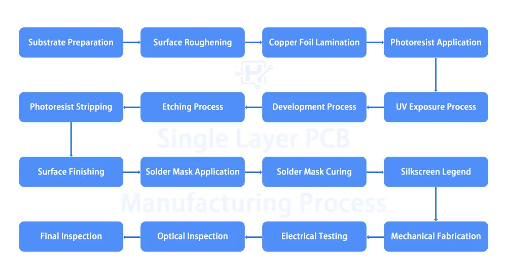
1. Substrate Preparation and Initial Processing
The single layer PCB manufacturing process begins with substrate preparation, forming the foundation for subsequent operations. High-quality fiberglass substrate material undergoes thorough cleaning to remove contaminants and ensure optimal copper adhesion. Surface treatment processes create the ideal bonding environment between substrate and copper foil.
| Process Step | Purpose | Quality Standards |
|---|---|---|
| Substrate Cleaning | Remove organic and inorganic contaminants | Surface resistivity >10¹² Ω |
| Surface Roughening | Enhance copper adhesion | Ra 0.5–2.0 μm |
| Adhesion Treatment | Promote chemical bonding | Bond strength >1.2 N/mm |
2. Copper Foil Application and Bonding
Professional copper foil application involves precise lamination processes under controlled temperature and pressure conditions. The copper foil, typically ranging from 0.5 to 2.0 ounces per square foot, bonds permanently to the substrate through heat and pressure application. This critical step determines the electrical performance and reliability of the finished PCB.
3. Photolithography and Pattern Transfer
The photolithography process transfers the circuit pattern from design files to the copper surface with exceptional precision. This multi-step procedure includes photoresist application, exposure through photomasks, and development processes that create the exact circuit patterns required.
Photoresist Application Techniques
Modern single layer PCB manufacturing employs advanced photoresist application methods to ensure uniform coverage and optimal resolution. Spin coating or curtain coating techniques apply photoresist layers with precise thickness control, typically maintaining variations within ±10% across the entire panel surface.
Exposure and Development Parameters
UV exposure systems utilize specific wavelengths and energy densities to create accurate pattern transfer. Development processes remove either exposed or unexposed photoresist areas, depending on the resist type, revealing the desired copper pattern for subsequent etching operations.
Advanced Manufacturing Techniques and Quality Control
1. Precision Etching and Copper Removal
The etching process removes unwanted copper material while preserving the desired circuit patterns. Chemical etching solutions dissolve exposed copper areas, leaving protected regions intact under the photoresist layer. Process control parameters include solution concentration, temperature, agitation rate, and contact time.
Etching Chemistry and Process Control
Professional PCB manufacturers utilize various etching solutions depending on production requirements and environmental considerations. Ferric chloride, ammonium persulfate, and alkaline solutions each offer specific advantages for different applications. Precise control of etching parameters ensures consistent line width, spacing, and copper thickness across production batches.
2. Surface Finishing and Protection
Post-etching processes prepare the PCB surface for component assembly and environmental protection. Surface finishing options include:
- Hot Air Solder Leveling (HASL): Provides excellent solderability and cost-effective protection
- Electroless Nickel Immersion Gold (ENIG): Offers superior flatness and long-term reliability
- Organic Solderability Preservative (OSP): Delivers environmental protection with minimal thickness addition
- Immersion Silver: Combines good electrical properties with cost efficiency
3. Solder Mask Application and Curing
Solder mask application protects copper traces from oxidation and prevents solder bridging during assembly operations. Modern liquid photoimageable solder masks provide excellent resolution and durability through precise application and UV curing processes.
Silkscreen Legend and Component Identification
The final manufacturing step applies silkscreen legends that provide component identification, polarity markers, and assembly instructions. This process uses specialized inks and curing methods to ensure permanent marking that withstands assembly and operational environments.

Quality Assurance and Testing Protocols
1. Electrical Testing and Verification
Comprehensive electrical testing validates single layer PCB functionality and reliability. Automated test equipment performs continuity checks, insulation resistance measurements, and impedance verification to ensure compliance with design specifications.
Visual Inspection and Defect Analysis
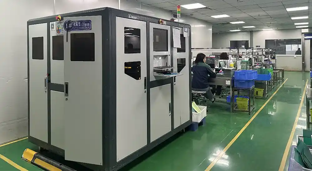
Professional quality control includes detailed visual inspection using automated optical inspection (AOI) systems. These systems detect various defects including:
- Copper thickness variations and incomplete etching
- Solder mask alignment and coverage issues
- Silkscreen registration and clarity problems
- Surface contamination and handling damage
2. Dimensional Accuracy and Mechanical Properties
Precision measurement systems verify dimensional accuracy, hole positions, and mechanical properties. Coordinate measuring machines and optical measurement systems ensure compliance with engineering drawings and industry standards.
| Step | Process Stage | Process Description | Key Parameters |
|---|---|---|---|
| 1 | Substrate Preparation | Clean substrate material to remove contaminants and ensure optimal copper foil adhesion environment | Surface resistivity >1012 Ω |
| 2 | Surface Roughening | Enhance copper foil adhesion to substrate through mechanical or chemical surface treatment | Ra 0.5–2.0 μm |
| 3 | Copper Foil Lamination | Permanently bond copper foil to substrate under controlled temperature and pressure conditions | 0.5–2.0 oz/sq ft |
| 4 | Photoresist Application | Apply uniform photoresist coating to prepare for pattern transfer processes | Thickness variation ±10% |
| 5 | UV Exposure Process | Transfer circuit patterns precisely to copper surface through photomask exposure | UV energy density control |
| 6 | Development Process | Remove exposed or unexposed photoresist areas to reveal desired copper patterns | Development time and temperature control |
| 7 | Etching Process | Chemically dissolve unwanted copper material while preserving photoresist-protected circuit patterns | Solution concentration, temperature, contact time |
| 8 | Photoresist Stripping | Remove remaining photoresist material to expose completed copper circuit patterns | Stripping solution concentration and time |
| 9 | Surface Finishing | Apply surface coating to protect copper traces and provide solderability | Coating thickness and uniformity |
| 10 | Solder Mask Application | Apply solder mask ink to protect copper traces from oxidation and prevent solder bridging | Coating thickness and adhesion |
| 11 | Solder Mask Curing | UV cure solder mask material to form permanent protective layer | UV curing energy and time |
| 12 | Silkscreen Legend | Print component identification, polarity markers, and assembly instructions | Print accuracy and clarity |
| 13 | Mechanical Fabrication | Cut PCB outline and drill holes according to design requirements | Dimensional accuracy ±0.1mm |
| 14 | Electrical Testing | Perform continuity testing, insulation resistance, and impedance verification | Test per design specifications |
| 15 | Optical Inspection | Use AOI systems to detect various defects and quality issues | Detection accuracy and coverage |
| 16 | Final Inspection | Dimensional measurement, mechanical properties, and visual quality inspection | Compliance with engineering drawings |
Conclusion: Choosing Professional PCB Manufacturing
The manufacturing of single layer PCBs requires meticulous attention to detail, advanced equipment, and stringent quality control at every stage. From material selection to final inspection, consistent product performance depends on experienced technicians and reliable processes.
If you’re looking for dependable single layer PCB manufacturing, working with a proven partner can make all the difference. Haoyue Electronics offers end-to-end PCB manufacturing and assembly services tailored to your unique project needs. Our expertise ensures not only manufacturing precision but also long-term reliability and cost efficiency.
With state-of-the-art facilities and a seasoned engineering team, we support your project from design optimization through production and final assembly. Whether you’re building consumer devices, LED systems, or industrial controls, we’re here to help you succeed.
Ready to bring your PCB design to life?
Contact our technical experts today to learn how Haoyue Electronics can support your next project with professional-grade single layer PCB solutions.
FAQ
1. What is the typical copper thickness used in single layer PCB manufacturing?
In single layer PCB manufacturing, the copper thickness typically ranges from 0.5 oz to 2.0 oz per square foot, depending on the current-carrying requirements of the circuit. Thicker copper layers are used for power PCBs or thermal-critical applications, while standard signal circuits often use 1.0 oz copper for cost efficiency and sufficient conductivity.
2. What are the advantages of using a single layer PCB over a multilayer PCB?
Single layer PCBs are favored for their low manufacturing cost, simple design process, and faster production turnaround. They’re ideal for applications where circuit complexity is low, such as in LED lighting, consumer electronics, and prototyping boards. Compared to multilayer PCBs, they also have fewer potential failure points and are easier to inspect and repair.
3. Can single layer PCBs support surface mount technology (SMT)?
Yes, single layer PCBs can fully support SMT PCB assembly. Although all components and traces are on the same side, modern SMT techniques allow for high-density layouts even on single layer boards. Proper design considerations—like trace routing and pad spacing—are crucial to avoid shorts and ensure manufacturing reliability.
4. How do I choose a reliable single layer PCB manufacturer in China?
When selecting a single layer PCB manufacturer in China, look for companies with ISO certifications, in-house fabrication and assembly capabilities, and a strong record of quality assurance. Ask for manufacturing process videos, sample testing reports, and customer references to validate their expertise. Haoyue Electronics provides professional one-stop PCB manufacturing services with strict quality standards and technical support throughout your project.

