The strategic implementation of rigid-flex PCB stackups requires comprehensive understanding of material science, mechanical engineering principles, and electrical performance optimization. As electronic devices continue to miniaturize while demanding enhanced functionality, mastering rigid-flex stackup design becomes essential for competitive advantage in today’s technology landscape.
Rigid-Flex PCB Stackup Fundamentals and Architecture
Core Construction Principles
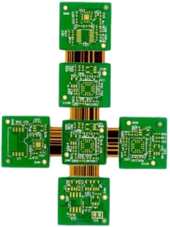
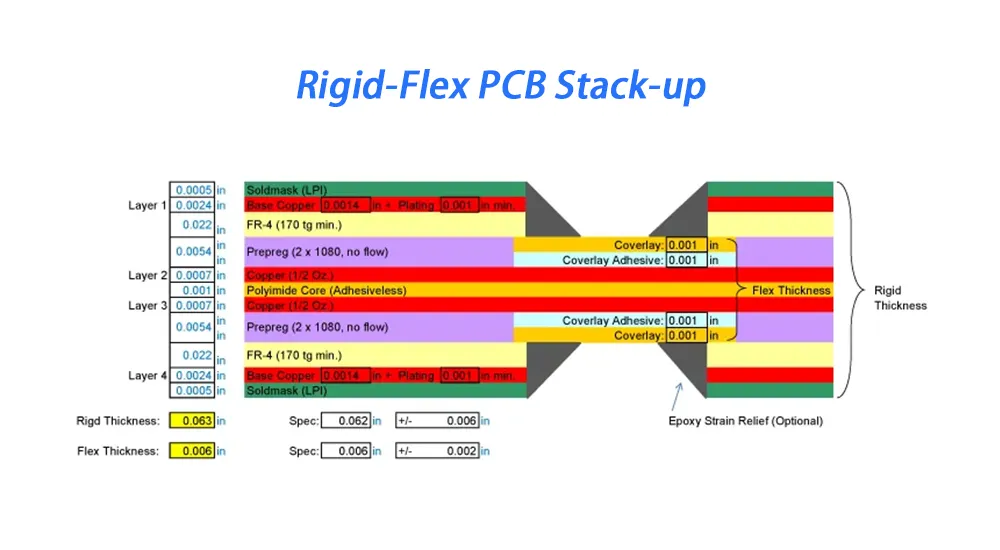
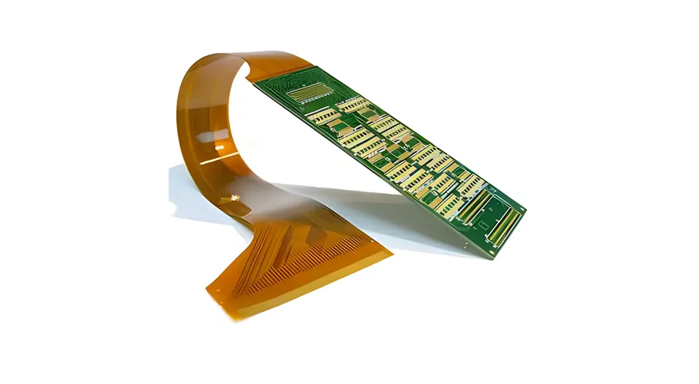
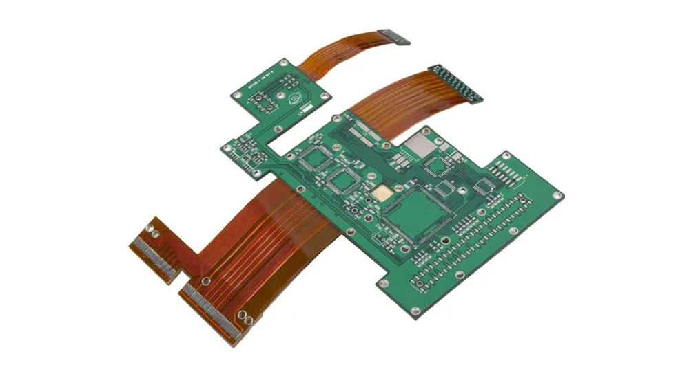
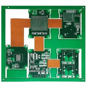
Rigid-flex PCB stackup architecture fundamentally differs from conventional printed circuit boards through its heterogeneous material composition and three-dimensional design capability. The architecture consists of alternating rigid and flexible sections that are permanently bonded during the lamination process, creating a single integrated circuit assembly.
The construction methodology involves rigid sections that utilize FR-4 or high-performance polyimide substrates, providing mechanical support for component mounting and heat dissipation. These areas accommodate standard surface-mount and through-hole components while maintaining dimensional stability under thermal cycling and mechanical stress. The transition zones between rigid and flexible sections require careful engineering to prevent stress concentration and ensure reliable electrical continuity throughout the operating lifecycle.
Flexible sections employ specialized polyimide films, commonly ranging from 12 to 125 micrometers in thickness, depending on bend radius requirements and layer count. The copper conductors in flexible regions utilize rolled annealed copper for superior flexibility and fatigue resistance compared to electrodeposited copper used in rigid sections.
Material Composition and Integration
The strategic arrangement of materials in rigid-flex PCB stackups directly influences both performance characteristics and manufacturing feasibility. The construction involves multiple specialized materials, each selected for specific performance requirements:
| Material Type | Thickness Range (μm) | Primary Applications | Key Properties |
|---|---|---|---|
| Rigid Substrate (FR-4) | 200–3200 | Component mounting, high-density routing | High strength, thermal stability |
| Flexible Polyimide | 12–125 | Dynamic flexing, space-constrained routing | Excellent flexibility, chemical resistance |
| Adhesive Layers | 12–25 | Material bonding, stress distribution | Temperature resistance, adhesion strength |
| Copper Foil | 9–70 | Electrical conductivity | High conductivity, bend fatigue resistance |
Adhesive interfaces create permanent bonds between dissimilar materials while accommodating thermal expansion differences that occur during operation and manufacturing processes. Advanced designs may incorporate adhesiveless constructions using specialized polyimide films with integral bonding capabilities, eliminating potential delamination points and reducing overall stackup thickness.
Electrical Performance and Signal Integrity
The integration of electrical and mechanical requirements in rigid-flex PCB stackup design requires sophisticated engineering approaches that balance competing demands for electrical performance and mechanical flexibility. Impedance control becomes particularly challenging due to varying dielectric constants and thicknesses between rigid and flexible sections. Careful trace width adjustment and ground plane management ensure consistent impedance throughout signal paths, preventing reflections and crosstalk that can compromise system performance.
Signal integrity considerations extend beyond traditional PCB design challenges to encompass the dynamic behavior of conductors under flexing conditions. The mechanical stress management requires optimizing bend radius specifications and stress distribution patterns to prevent conductor fatigue and maintain long-term reliability. Thermal considerations become critical in rigid-flex designs where heat generation and dissipation characteristics vary significantly between sections.
Advanced Design Considerations and Material Selection
Layer Configuration Strategy
Strategic layer arrangement in rigid-flex stackups significantly influences both electrical performance and mechanical reliability. The optimal configuration balances signal routing requirements, power distribution needs, and flexing performance while minimizing manufacturing complexity and cost. Layer count determination involves analyzing multiple factors including signal routing density, power distribution requirements, and mechanical constraints.
The selection process must consider the exponential increase in manufacturing complexity and cost as layer count increases, while ensuring adequate functionality for the target application:
- 2-4 layers: Consumer electronics, simple medical devices, cost-sensitive applications
- 6-8 layers: Automotive electronics, industrial controls, moderate complexity designs
- 10-12 layers: Aerospace applications, high-performance computing, advanced telecommunications
- 14+ layers: Complex avionics, military systems, specialized high-density applications
Symmetrical stackups provide superior dimensional stability and reduce warpage tendencies during thermal processing. The configuration offers balanced thermal expansion characteristics that reduce stress-induced warpage during temperature cycling, resulting in more predictable mechanical behavior that simplifies stress analysis and reliability prediction. Asymmetrical designs may be necessary for specific functional requirements but require careful material selection and thickness balancing to prevent board distortion and delamination risks.
Advanced Material Selection Criteria
High-performance rigid-flex PCB stackup designs require careful evaluation of substrate material characteristics that extend beyond basic electrical and mechanical properties. Advanced polyimide substrates offer superior electrical properties and dimensional stability but require specialized processing techniques that may impact manufacturing schedules and costs.
Critical material parameters include dielectric constant specifications that typically range from 3.2 to 3.5 for standard polyimide materials, while specialized low-loss materials can achieve values below 3.0 with correspondingly reduced loss tangents. These electrical properties become critical for high-frequency applications where signal integrity directly impacts system performance. Loss tangent characteristics range from 0.002 to 0.008 depending on material formulation and processing techniques.
Thermal expansion coefficient matching between rigid and flexible sections prevents stress-induced failures during thermal cycling operations. The coefficient of thermal expansion for polyimide typically measures 12–16 ppm/°C in the machine direction and 16–20 ppm/°C in the transverse direction, requiring careful consideration during stackup design to minimize stress concentration at material interfaces.
Via Technology and Interconnection Methods
Via technology in rigid-flex PCB stackup designs encompasses multiple categories, each serving specific interconnection requirements while presenting unique manufacturing challenges and design constraints. Through-hole vias provide the most reliable interconnection method but consume significant board area and may limit flexible section bend radius capabilities. Mechanical drilling processes typically limit minimum via sizes to approximately 100 micrometers, while laser drilling enables smaller geometries down to 25 micrometers for high-density applications.
Blind and buried via structures enable higher interconnect density while preserving flexible section properties, though they require sequential lamination processes that increase manufacturing complexity and costs. These advanced via types demand precision depth control to ensure reliable connections without compromising adjacent layers, while offering enhanced design flexibility through improved routing options and potential layer count reductions.
Manufacturing Process and Quality Control
Advanced Fabrication Techniques
Modern rigid-flex PCB stackup manufacturing employs sophisticated lamination processes that precisely control temperature, pressure, and atmospheric conditions to achieve optimal inter-layer bonding. The fabrication workflow begins with material preparation, including substrate cutting, copper surface treatment, and adhesive application, all requiring precision techniques to prevent delamination and ensure accurate dimensional control.
Lamination processes represent the most critical manufacturing step, requiring precise parameter control across multiple variables:
- Temperature control: 185°C to 220°C depending on material system, maintained within ±3°C tolerance
- Pressure application: 200–400 PSI with uniform distribution across complex geometries
- Cycle time optimization: 60–120 minutes based on thickness and material requirements
- Atmospheric control: Vacuum or inert gas environments to prevent oxidation and void formation
Surface preparation techniques significantly enhance bond strength between dissimilar materials through controlled mechanical and chemical modification. Plasma treatment modifies surface energy characteristics and improves wetting properties, while chemical etching creates controlled surface roughening that enhances mechanical interlocking between layers. Corona treatment provides cost-effective surface modification for high-volume applications, and specialized primer application utilizes coupling agents for the most demanding applications.
Quality Control and Testing Protocols
Quality control protocols for rigid-flex PCB stackups extend beyond standard printed circuit board testing to encompass the unique characteristics and failure modes associated with flexible circuit technology. Electrical performance validation includes dynamic impedance testing that characterizes performance under flexing conditions, conductor resistance monitoring that provides real-time measurement during flex cycling, and insulation resistance verification through high-voltage testing across material interfaces.
Mechanical reliability assessment validates both immediate performance and long-term reliability under operational conditions through comprehensive testing protocols. Flex life testing represents a critical validation step that includes several key parameters:
- Standard test conditions: Room temperature, 50% relative humidity
- Bend radius specifications: Typically 6–10 times overall thickness
- Cycling frequency: 60–120 cycles per minute for accelerated testing
- Failure criteria: 10% increase in conductor resistance or visible damage
Environmental stress testing encompasses temperature cycling from -55°C to +125°C with controlled ramp rates, humidity testing at elevated temperature and humidity conditions for extended periods, vibration testing including both sinusoidal and random vibration profiles, and chemical resistance evaluation through exposure to process chemicals and operating fluids.
Manufacturing Process Optimization
Process monitoring and feedback systems in advanced manufacturing facilities ensure consistent quality and optimize production efficiency. Real-time temperature monitoring provides thermal profiling throughout lamination cycles, while pressure distribution analysis ensures uniform bonding across complex geometries. Material handling automation minimizes contamination and handling damage, and statistical process control enables continuous improvement through comprehensive data analysis.
Manufacturing yield optimization requires systematic analysis of failure modes and implementation of preventive measures. Design for manufacturability principles guide early collaboration between design and manufacturing teams, while process capability studies provide statistical analysis of process variation and control limits. Failure mode analysis enables root cause investigation and corrective action implementation, supported by continuous improvement programs that drive regular process optimization and technology upgrades.
Applications and Industry Trends
Aerospace and Military Electronics
Rigid-flex PCB stackups are widely used in aerospace for mission-critical systems that demand high reliability, lightweight construction, and resistance to harsh environments.
Key applications include:
- Flight control computers
- Navigation and communication systems
- Satellite systems with radiation resistance and low outgassing
- Military-grade electronics with extended temperature and shock resistance
Medical Devices
Medical applications benefit from the compact, biocompatible, and flexible nature of rigid-flex PCBs. Common use cases include:
- Implantable devices: Pacemakers, neurostimulators, drug delivery systems
- Diagnostic equipment: Ultrasound probes, endoscopes, portable analyzers
- Surgical tools: Robotic instruments, minimally invasive tools
- Wearables: Health monitors, bio-signal sensors for patient comfort
Automotive Applications
Rigid-flex designs are increasingly adopted in automotive electronics, especially for:
- Advanced driver assistance systems (ADAS)
- Radar and camera modules
- Sensor fusion units
- Electric vehicle (EV) power systems
Emerging Technology Trends
Advanced Materials
Innovation in materials continues to expand rigid-flex capabilities:
- Low-loss dielectrics for high-frequency signal performance
- Thermally conductive substrates for better heat dissipation
- Improved mechanical strength and flex-life performance
Next-Gen Integration
Rigid-flex is evolving alongside other electronics manufacturing trends:
- Embedded components within the substrate
- Additive manufacturing of complex 3D circuit structures
- Flexible hybrid electronics (FHE) integration
- Printed electronics for sensors and miniaturized systems
Market Outlook
Industry projections show an 8–12% CAGR through 2030.
Driving forces include:
- Lower costs and design tool advancements
- Mass production readiness
- Cross-industry adoption in medical, automotive, consumer electronics, and aerospace
Sustainable Development
Future trends will emphasize:
- Recyclable materials and green substrates
- System-in-package (SiP) integration
- Reduced environmental impact throughout the product lifecycle
Partner with Haoyue Electronics for Advanced Rigid-Flex PCB Solutions
Haoyue Electronics specializes in manufacturing high-quality rigid-flex PCB stackups that meet the most demanding technical specifications across aerospace, medical, automotive, and consumer electronics applications. Our state-of-the-art manufacturing facilities and experienced engineering team ensure your designs achieve optimal performance, reliability, and cost-effectiveness.
From prototype development through high-volume production, we provide comprehensive support throughout your project lifecycle, including design optimization, material selection guidance, and extensive quality validation. Our commitment to continuous improvement and advanced manufacturing technologies positions us as your trusted partner for innovative rigid-flex PCB solutions.
Contact our technical team today to discuss your specific rigid-flex PCB requirements and discover how our advanced manufacturing capabilities and engineering expertise can accelerate your product development while ensuring superior performance outcomes.

