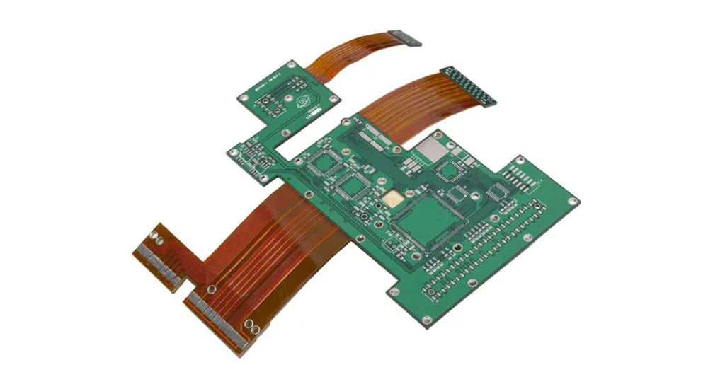
Rigid-flex PCB design represents one of the most sophisticated approaches to modern electronic packaging, combining the structural integrity of rigid boards with the flexibility of flex circuits. This hybrid technology enables designers to create three-dimensional electronic assemblies that reduce connector failures, minimize assembly time, and optimize space utilization in complex electronic systems.
The evolution of rigid-flex technology has transformed industries ranging from aerospace and medical devices to consumer electronics and automotive applications. Understanding the intricate design requirements, material science, and manufacturing constraints is essential for engineers seeking to leverage the full potential of rigid-flex PCB solutions.
Understanding Rigid-Flex PCB Technology and Design Fundamentals
Core Architecture and Stackup Design
Rigid-flex PCB design fundamentally differs from traditional rigid board design due to its multi-zone architecture. The stackup consists of alternating rigid and flexible sections, with specific layer arrangements that must maintain electrical continuity while accommodating mechanical stress.
The typical rigid-flex stackup includes coverlay or coverlays in flex regions, adhesive layers for lamination, and copper foil patterns that extend seamlessly between rigid and flexible zones. The transition zones between rigid and flexible sections require careful consideration of material properties and thickness variations to prevent stress concentrations that could lead to failure.
Material Selection and Properties
Material selection forms the foundation of successful rigid-flex PCB design. Polyimide remains the preferred substrate material for flexible sections due to its excellent thermal stability, chemical resistance, and mechanical properties. The dielectric constant and loss tangent characteristics of polyimide must be carefully matched with the rigid section materials to maintain impedance control across the entire circuit.
Adhesive systems play a critical role in rigid-flex construction. Acrylic adhesives offer superior flexibility and temperature resistance, while modified epoxy systems provide enhanced adhesion strength for high-reliability applications. The selection between adhesive and adhesiveless construction impacts both electrical performance and mechanical reliability.
Electrical Design Considerations
Impedance control in rigid-flex designs requires sophisticated modeling that accounts for the different dielectric properties between rigid and flexible sections. The impedance discontinuities at transition zones must be minimized through careful trace geometry optimization and stackup design.
Signal integrity considerations extend beyond traditional rigid board design requirements. The dynamic flexing of cable sections introduces unique challenges for high-speed digital signals, requiring attention to differential pair routing, ground plane continuity, and via placement strategies.
Critical Design Requirements and Material Considerations
Bend Radius and Mechanical Constraints
The minimum bend radius represents one of the most critical design constraints in rigid-flex PCB design. The bend radius must be calculated based on the total thickness of the flexible section, including all copper layers, dielectric materials, and coverlays. Industry standards typically require a minimum bend radius of 6 to 10 times the total thickness for static applications, while dynamic flexing applications may require 20 times or greater.
Layer Count and Thickness Management
Layer count optimization in flexible regions directly impacts both cost and reliability. Each additional copper layer increases the minimum bend radius and reduces flexibility. Strategic layer planning often involves redistributing routing to rigid sections where possible, minimizing the copper density in flex regions.
| Flex Layer Count | Typical Thickness | Min Bend Radius (Static) | Min Bend Radius (Dynamic) |
|---|---|---|---|
| 1 Layer | 0.1-0.2mm | 1.0-2.0mm | 3.0-6.0mm |
| 2 Layer | 0.2-0.3mm | 2.0-3.0mm | 6.0-9.0mm |
| 4 Layer | 0.4-0.6mm | 4.0-6.0mm | 12.0-18.0mm |
| 6+ Layer | 0.8mm+ | 8.0mm+ | 24.0mm+ |
Environmental and Reliability Requirements
Rigid-flex PCBs must withstand diverse environmental conditions including temperature cycling, vibration, and humidity exposure. The coefficient of thermal expansion mismatch between rigid and flexible materials creates stress concentrations that must be addressed through proper design techniques.
Reliability testing protocols for rigid-flex assemblies include accelerated life testing, bend cycling, and thermal shock testing. These tests validate the design approach and material selection for specific application requirements.
Layout Principles and Routing Strategies for Rigid-Flex PCBs
Transition Zone Design
The transition between rigid and flexible sections requires meticulous attention to stress relief and copper pattern design. Teardrop connections at via locations provide stress relief and improve the reliability of plated through holes that span rigid-flex boundaries.
Copper balancing across the flex region prevents the formation of stress concentrations during flexing. Hatched copper fills or crosshatched ground planes distribute mechanical stress more effectively than solid copper pours, which can create stress risers at pattern edges.
Trace Routing Optimization
Trace routing in flexible sections follows specific principles that differ from rigid board design practices. Curved traces are preferred over angled traces to distribute stress more evenly during flexing. The preferred approach involves using arc-shaped routing with smooth transitions rather than sharp angular changes.
Via Design and Placement
Via placement in rigid-flex designs requires strategic planning to ensure mechanical integrity and electrical performance. Vias should be positioned in rigid sections whenever possible, as the drilling and plating processes can create stress concentrations in flexible materials.
When vias must be placed in or near flexible sections, additional design considerations include:
- Increased via pad sizes to accommodate manufacturing tolerances
- Via filling or plugging to prevent plating solution entrapment
- Strategic placement away from maximum stress areas
- Use of microvias for reduced mechanical impact
Component Placement Strategy
Component placement on rigid-flex assemblies requires coordination between mechanical and electrical design requirements. Components must be positioned to avoid interference with flexing sections while maintaining optimal electrical performance and thermal management.
The placement of components near rigid-flex transition zones requires special attention to mechanical stress transfer. Standoff components and stress-relief features may be necessary to prevent mechanical coupling between rigid sections during flexing operations.
Common Design Challenges and Solutions
Impedance Control Across Transitions
Maintaining consistent impedance across rigid-flex transitions presents significant challenges due to material property variations and manufacturing tolerances. Advanced electromagnetic simulation tools are essential for predicting and optimizing impedance behavior across the entire signal path.
Compensation techniques include local trace width adjustments, ground plane modifications, and strategic via placement to minimize impedance discontinuities. These techniques require close collaboration between design and manufacturing teams to ensure manufacturability.
Manufacturing Yield Optimization
Design for manufacturability principles take on heightened importance in rigid-flex PCB design due to the complexity of the manufacturing process. Critical design reviews should address panelization strategies, drilling considerations, and inspection accessibility.
Key yield optimization strategies include:
- Adequate tooling hole placement for manufacturing alignment
- Proper panel design to minimize material waste
- Consideration of inspection and testing accessibility
- Coordination of assembly and manufacturing processes
Thermal Management Considerations
Thermal management in rigid-flex assemblies requires careful consideration of heat dissipation paths and thermal expansion effects. The limited thermal conductivity of polyimide materials necessitates strategic component placement and thermal interface design.
Thermal vias and heat spreading techniques must be implemented without compromising the mechanical flexibility of the design. Advanced thermal simulation tools help optimize the balance between thermal performance and mechanical reliability.
Cost Optimization Strategies
Rigid-flex PCB costs can be significantly higher than traditional rigid board solutions, making cost optimization a critical design consideration. Effective cost management strategies include minimizing flex region area, optimizing layer counts, and standardizing bend geometries.
Material utilization efficiency becomes particularly important due to the specialized nature of flex materials. Panel optimization and material waste reduction directly impact overall project costs.

Manufacturing Considerations and Best Practices
Design Rule Validation and DFM Analysis
Comprehensive design rule checking specific to rigid-flex technology ensures manufacturability and reliability. Standard PCB design rules are insufficient for rigid-flex applications, requiring specialized rule sets that address the unique constraints of flexible circuit manufacturing.
Manufacturing partners play a crucial role in design validation, providing expertise in material selection, process capabilities, and yield optimization. Early engagement with manufacturing partners, such as experienced companies like Haoyue Electronics, enables design optimization based on actual production capabilities and constraints.
Assembly Process Integration
The assembly process for rigid-flex PCBs requires specialized handling and fixturing to prevent damage during component placement and soldering operations. The design must accommodate assembly tooling requirements while maintaining the intended mechanical functionality.
Selective soldering processes may be required for assemblies where flexing occurs near populated areas. Component placement must consider both initial assembly requirements and long-term reliability under dynamic flexing conditions.
Quality Assurance and Testing Protocols
Quality assurance for rigid-flex assemblies encompasses both electrical testing and mechanical validation. In-circuit testing strategies must account for the three-dimensional nature of the assembled product and potential access limitations.
Mechanical testing protocols validate the bend performance and fatigue life of the assembly under operational conditions. These tests are essential for qualifying the design for its intended application environment.
Partner with Haoyue Electronics for Advanced Rigid-Flex Solutions
Successful rigid-flex PCB design requires the integration of advanced engineering expertise with proven manufacturing capabilities. Haoyue Electronics brings decades of experience in rigid-flex PCB manufacturing and assembly, offering comprehensive design support from initial concept through production validation.
Our engineering team collaborates closely with customers to optimize designs for manufacturability while meeting performance requirements and cost targets. With state-of-the-art manufacturing facilities and rigorous quality control processes, Haoyue Electronics delivers reliable rigid-flex solutions for demanding applications across aerospace, medical, and high-technology industries.
Contact our technical team to discuss your rigid-flex PCB design requirements and discover how our expertise can accelerate your product development timeline while ensuring optimal performance and reliability.

