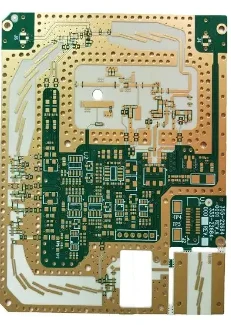
The complexity of RF circuit design necessitates a thorough understanding of how electromagnetic fields interact with PCB substrates, conductor patterns, and surrounding environments. Engineers must balance multiple competing factors including insertion loss, return loss, crosstalk, and thermal management while meeting stringent performance specifications.
Understanding RF PCB Characteristics Fundamentals
RF PCB design differs significantly from standard digital circuit boards due to the unique behavior of high-frequency signals. At RF frequencies, traditional circuit analysis methods become inadequate, and electromagnetic field theory governs circuit performance.
Critical Parameters in RF Design
Signal wavelength becomes comparable to physical dimensions of circuit elements at RF frequencies. This relationship fundamentally alters how signals propagate through the PCB structure. Parasitic capacitances and inductances that remain negligible at lower frequencies become dominant factors affecting circuit behavior.
Transmission Line Effects
RF circuits must be analyzed as transmission line structures rather than simple lumped element circuits. Characteristic impedance, propagation constant, and reflection coefficient become primary design parameters. Understanding these RF PCB characteristics enables engineers to predict and control signal behavior throughout the frequency spectrum.
Dielectric Materials and Their Impact on RF Performance
The selection of dielectric materials represents one of the most critical decisions in RF PCB design. Material properties directly influence signal propagation characteristics, power handling capabilities, and overall circuit performance.
Dielectric Constant Considerations
Low dielectric constant materials reduce signal propagation delay and minimize dielectric losses. However, achieving consistent dielectric properties across frequency and temperature ranges requires careful material selection. Advanced RF substrates like Rogers RO4000 series, Taconic TLY, and Isola I-Tera MT provide superior performance compared to standard FR4 materials.
The dielectric constant tolerance significantly impacts impedance control accuracy. High-frequency applications typically require materials with dielectric constant tolerances of ±0.02 or better. This precision enables maintaining characteristic impedance within ±5% across the entire PCB.
Loss Tangent and Quality Factor
Dielectric loss tangent directly affects insertion loss and signal integrity. Low-loss materials with tan δ values below 0.002 at RF frequencies minimize signal attenuation and reduce power consumption. The relationship between loss tangent and frequency determines the practical upper frequency limits for each material system.
Advanced ceramic-filled PTFE composites offer exceptional electrical performance with loss tangent values as low as 0.0009 at 10 GHz. These materials enable the design of high-Q resonant structures and low-noise amplifier circuits with superior performance characteristics.
Thermal Coefficient of Dielectric Constant
Temperature stability of dielectric properties affects circuit performance across operating temperature ranges. Materials with low thermal coefficients of dielectric constant maintain consistent electrical characteristics, reducing frequency drift and impedance variations in temperature-sensitive applications.

RF PCB
Impedance Control and Signal Integrity
Precise impedance control forms the foundation of successful RF PCB design. Maintaining target characteristic impedance values requires careful control of trace geometry, dielectric thickness, and material properties.
Trace Geometry Optimization
Microstrip and stripline configurations each offer distinct advantages for different applications. Microstrip provides easier component placement and lower fabrication costs, while stripline offers superior isolation and reduced electromagnetic interference.
Critical dimensions including trace width, dielectric thickness, and ground plane separation must be controlled within tight tolerances. Typical impedance control requirements for RF applications demand ±5% or better accuracy across the entire PCB.
Via Design and Optimization
Via structures create discontinuities in RF transmission paths, causing reflections and impedance mismatches. Optimizing via diameter, pad size, and anti-pad dimensions minimizes these effects. Advanced via-in-pad and microvias enable high-density routing while maintaining signal integrity.

RF PCB Manufacturing
High-Frequency Design Challenges and Solutions
RF PCB design presents unique challenges that require specialized solutions and deep understanding of electromagnetic principles.
Ground Plane Design
Solid ground planes provide current return paths and electromagnetic shielding. Proper ground plane design minimizes ground bounce, reduces electromagnetic interference, and maintains consistent reference potentials for RF circuits.
Component Placement and Routing
Strategic component placement minimizes parasitic coupling and reduces unwanted interactions between circuit elements. Maintaining adequate spacing between sensitive circuits, implementing proper shielding techniques, and controlling current flow paths become essential for achieving target performance specifications.
Manufacturing Considerations for RF PCBs
Manufacturing precision directly impacts RF circuit performance. Standard PCB fabrication tolerances may prove inadequate for demanding high-frequency applications.
Fabrication Tolerances
RF applications typically require tighter manufacturing tolerances compared to standard digital circuits. Line width variations must be controlled within ±10% or better, while dielectric thickness tolerances of ±5% ensure consistent impedance characteristics.
Surface Finish Selection
Surface finish selection affects both electrical performance and assembly reliability. Immersion silver and ENIG (Electroless Nickel Immersion Gold) finishes provide excellent high-frequency characteristics while maintaining solderability for component assembly.
Haoyue Electronics: Advanced RF PCB Manufacturing Capabilities
Haoyue Electronics specializes in precision manufacturing of RF PCBs with exceptional attention to the critical characteristics that determine high-frequency performance. Our comprehensive capabilities address the demanding requirements of modern RF applications.
Our advanced manufacturing processes ensure consistent delivery of high-performance RF circuits that meet stringent electrical specifications. We understand that successful RF PCB implementation requires more than standard fabrication techniques.
Core RF Manufacturing Capabilities
- Impedance control within ±5% tolerance using advanced measurement techniques
- Support for low-loss RF materials including Rogers, Taconic, and Isola substrates
- Precision drilling and via formation optimized for high-frequency applications
- Advanced surface finishes designed for RF performance and assembly reliability
- Comprehensive electrical testing including time domain reflectometry and network analysis
- Complete PCB assembly services with RF-qualified components and specialized placement equipment
Our engineering team collaborates closely with customers to optimize RF PCB characteristics for specific application requirements. From initial design review through final testing and qualification, we provide comprehensive support for critical RF applications.
Contact Haoyue Electronics to discuss your RF PCB requirements and discover how our specialized capabilities can enhance your high-frequency circuit performance. Our expertise in RF PCB characteristics ensures successful implementation of your most demanding applications.

