Material Selection and Property Challenges
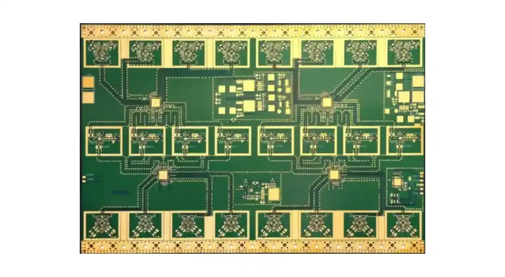
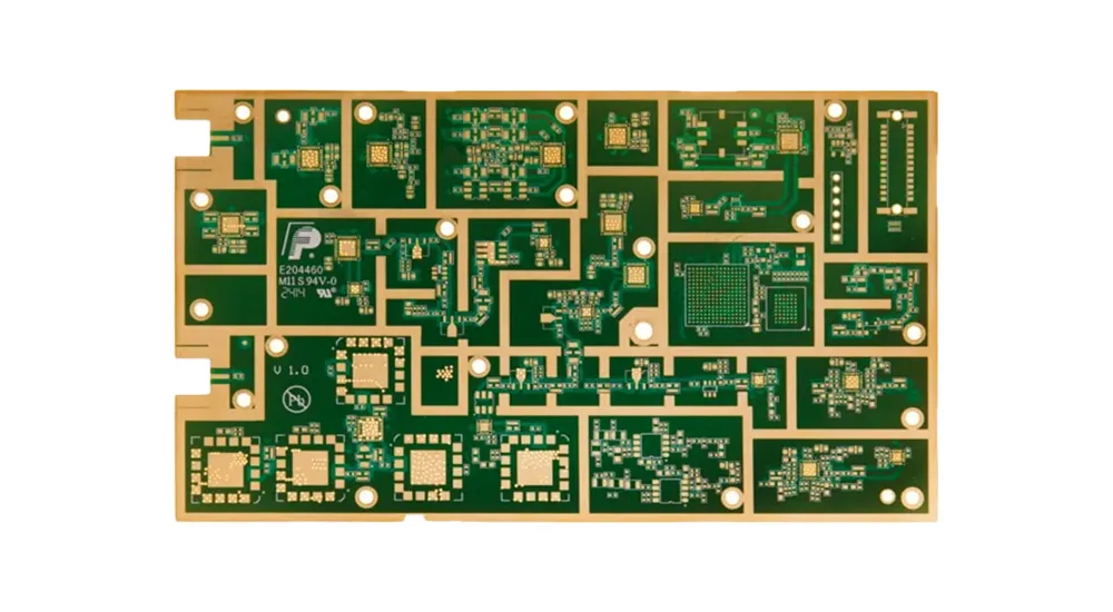
High-frequency PCB manufacturing begins with the fundamental challenge of material selection. Unlike standard FR4 substrates, RF and microwave applications demand specialized laminates that maintain consistent electrical properties across wide frequency ranges.
Dielectric Constant Stability Issues
The dielectric constant (Dk) of substrate materials must remain stable across temperature variations and frequency ranges. Manufacturing variations in material thickness or dielectric properties can cause impedance mismatches that result in signal reflection and loss. Rogers laminates, PTFE-based materials, and ceramic-filled substrates are commonly specified, but each presents unique handling and processing challenges during fabrication.
Loss Tangent Control Complexities
Maintaining low loss tangent (Df) values throughout the manufacturing process requires careful control of material moisture content, curing temperatures, and lamination pressures. Even slight deviations in processing parameters can increase dielectric losses, particularly problematic in high-power RF applications where signal integrity is paramount.
Thermal Management Material Integration
High-frequency circuits often require materials with enhanced thermal conductivity to manage heat dissipation. Integrating thermal management features like embedded heat spreaders or thermally conductive via fills adds complexity to the manufacturing process and requires specialized equipment and expertise.
Precision Manufacturing Requirements
The manufacturing tolerances required for RF and microwave PCBs far exceed those of conventional printed circuits. This section examines the critical precision challenges that manufacturers must overcome.
Controlled Impedance Manufacturing Tolerances
Achieving consistent characteristic impedance across an entire PCB requires maintaining extremely tight tolerances on trace width, substrate thickness, and dielectric properties. Production tolerances on high-frequency performance become critical when considering that a ±5% impedance variation can cause significant signal reflection at microwave frequencies.
The relationship between manufacturing precision and electrical performance is particularly evident in microstrip and stripline geometries. For 50-ohm impedance control, trace width variations of just ±0.0005 inches can result in impedance shifts of ±2 ohms or more, depending on the substrate thickness and dielectric constant. This level of precision demands advanced manufacturing capabilities including laser-controlled etching processes and continuous monitoring systems.
Layer-to-Layer Registration Accuracy
Multilayer RF PCBs require exceptional registration accuracy between layers to maintain via reliability and signal integrity. Misalignment between layers can create discontinuities in ground planes, affect via inductance, and introduce unwanted capacitive or inductive coupling between signal layers. Manufacturing processes must maintain registration tolerances of ±0.001 inches or better for critical high-frequency designs.
Surface Roughness Control Challenges
The surface roughness of copper traces significantly impacts high-frequency signal propagation due to the skin effect. At microwave frequencies, current flows primarily on the conductor surface, making surface finish critical for minimizing conductor losses. Manufacturing processes must carefully balance adhesion requirements with the need for smooth copper surfaces, often requiring specialized surface treatments or electroplating techniques.

RF & Microwave PCB
Laser Drilling and Via Formation Challenges
Modern RF PCB manufacturing increasingly relies on laser drilling technology to create precise microvias and maintain signal integrity in high-density interconnect designs.
Microvia Precision and Consistency
Laser drilling systems must achieve exceptional precision in via diameter, taper angle, and positional accuracy. For RF applications, via stub length becomes critical as it can create resonances that interfere with high-frequency signals. Manufacturing challenges include maintaining consistent laser power, controlling material removal rates, and achieving clean via sidewalls without thermal damage to surrounding materials.
Via Plating and Filling Complexities
Following laser drilling, the metallization and filling of microvias presents unique challenges. Proper via plating requires uniform copper deposition to maintain low resistance connections, while via filling techniques must eliminate voids that could cause reliability issues or affect electrical performance. The choice between conductive and non-conductive fill materials depends on specific electrical requirements and manufacturing capabilities.
Buried and Blind Via Manufacturing
Complex RF designs often require buried and blind vias to optimize signal routing and minimize layer count. Manufacturing these via structures demands precise control of drilling depth, accurate layer-to-layer registration, and specialized plating processes. The sequential lamination required for buried via construction introduces additional opportunities for manufacturing variations that can impact final performance.
Surface Treatment and Plating Complexities
Surface finishes and plating processes for RF PCBs must balance electrical performance requirements with manufacturability and reliability considerations.
High-Frequency Surface Finish Selection
Traditional HASL (Hot Air Solder Leveling) finishes are generally unsuitable for high-frequency applications due to surface roughness and thickness variations. Alternative finishes such as ENIG (Electroless Nickel Immersion Gold), OSP (Organic Solderability Preservative), or immersion silver each present specific manufacturing challenges while offering different electrical characteristics.
Thick Copper Electroplating Challenges
High-power RF applications often require thick copper plating to handle increased current density and improve thermal management. Manufacturing thick copper traces presents challenges in achieving uniform plating thickness, managing edge effects, and maintaining dimensional accuracy. Electroplating processes must be carefully controlled to prevent excessive buildup at trace edges while ensuring adequate thickness across the entire conductor width.
Selective Plating and Masking
Many RF designs require selective plating in specific areas to optimize performance or facilitate assembly processes. This requires precise masking techniques and multiple plating steps that increase manufacturing complexity and potential for defects. The registration accuracy between mask layers and circuit features becomes critical for maintaining design specifications.
Quality Control and Testing Challenges
Quality assurance for RF PCB manufacturing requires specialized testing equipment and procedures beyond those used for conventional printed circuits.
High-Frequency Electrical Testing
Vector Network Analyzers (VNA) and Time Domain Reflectometry (TDR) equipment are essential for verifying electrical performance at operational frequencies. These testing methods require specialized test fixtures, calibration procedures, and operator expertise. Manufacturing facilities must invest in expensive test equipment and maintain stringent calibration standards to ensure accurate measurements.
Production Line Integration Challenges
Integrating high-frequency testing into production workflows presents logistical challenges due to test complexity and duration. Automated test systems must be designed to handle the delicate nature of RF test fixtures while maintaining throughput requirements. The balance between comprehensive testing and production efficiency requires careful optimization of test procedures and sampling strategies.
Traceability and Documentation Requirements
RF PCB applications often require extensive documentation and traceability for materials, processes, and test results. This documentation burden increases manufacturing overhead while providing essential data for design optimization and failure analysis. Manufacturing systems must capture and maintain detailed records throughout the production process.
Haoyue Electronics: Advanced RF PCB Manufacturing Solutions
As a specialized PCB manufacturer and assembly provider, Haoyue Electronics has developed comprehensive capabilities to address the complex challenges inherent in RF and microwave PCB production. Our advanced manufacturing facility combines state-of-the-art equipment with experienced engineering expertise to deliver high-performance solutions for demanding applications.
Our Core RF Manufacturing Capabilities
Haoyue Electronics offers industry-leading capabilities specifically developed for high-frequency PCB manufacturing. Our laser drilling systems achieve via diameters down to 0.006 inches with exceptional positional accuracy, while our controlled impedance manufacturing processes maintain tolerances within ±5% across all frequency ranges.
Our surface treatment capabilities include multiple high-frequency compatible finishes, thick copper electroplating up to 4 oz/ft², and specialized selective plating processes. Advanced quality control systems utilizing VNA and TDR testing ensure every PCB meets stringent electrical specifications before delivery.
Comprehensive Assembly and Integration Services
Beyond PCB fabrication, our assembly capabilities encompass surface mount technology optimized for high-frequency components, precision soldering processes that maintain signal integrity, and complete system integration services. Our experienced engineering team provides design for manufacturability consultation to optimize designs for production efficiency while maintaining performance requirements.
Contact Haoyue Electronics today to discuss your RF and microwave PCB manufacturing requirements. Our technical team stands ready to transform your challenging designs into reliable, high-performance printed circuit solutions that meet the most demanding specifications.

