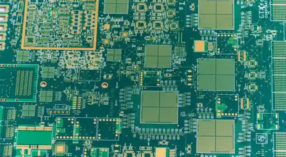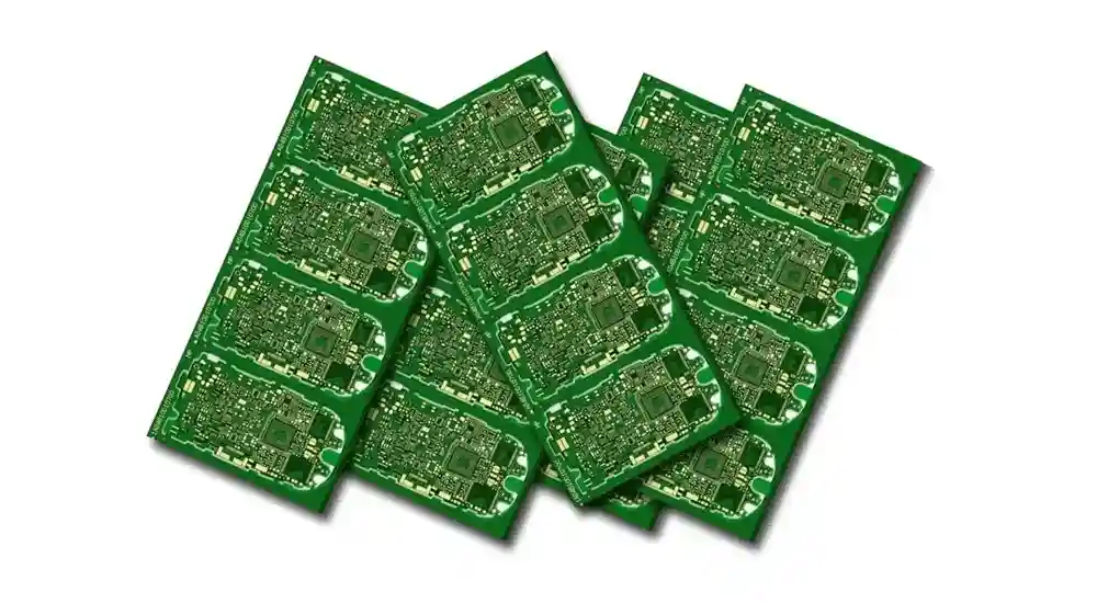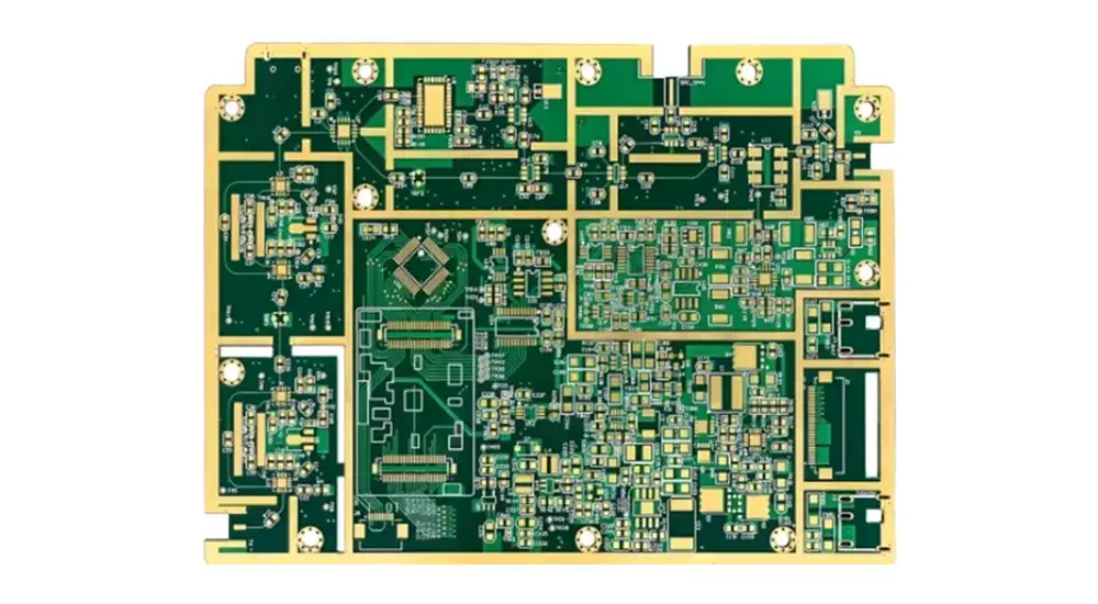
A multilayer PCB comprises three or more conductive copper layers separated by insulating dielectric materials, all laminated together under controlled conditions. This structure enables complex routing, superior signal integrity, improved power distribution, and effective electromagnetic interference control. Multilayer PCBs can range from standard four-layer designs to highly complex systems with up to 40 layers, each tailored to meet specific electrical and mechanical requirements.
Implementing effective multilayer PCB design principles directly enhances product performance, manufacturing yield, and long-term reliability. Understanding these principles is crucial for engineers developing next-generation products across industries such as telecommunications, automotive, aerospace, medical, and consumer electronics.
Layer Stackup Architecture and Strategic Planning
Fundamental Construction Principles
Multilayer PCB architecture follows specific structural principles that determine both electrical performance and manufacturing feasibility. The construction involves alternating conductive copper layers with dielectric prepreg materials, creating a unified laminated structure where core layers provide mechanical stability while prepreg layers serve as bonding agents during lamination.
The stackup configuration directly influences signal propagation characteristics, impedance control, and electromagnetic compatibility. Engineers must carefully balance signal layers, power planes, and ground planes to achieve optimal performance while maintaining cost-effectiveness.
Standard multilayer PCB stackup configurations include four-layer designs for moderate complexity applications, six to eight-layer arrangements for high-speed digital systems, and twelve or more layers for advanced processor boards and telecommunications equipment. Each configuration presents unique advantages and challenges that must be considered during the design phase.
Strategic Layer Function Assignment
The effectiveness of multilayer PCB design depends heavily on strategic layer function assignment based on circuit requirements and signal characteristics. This assignment process requires understanding how different layer types interact and influence overall system performance.
Signal layers accommodate high-speed digital traces, analog circuits, and RF transmission lines, with each layer optimized for specific impedance requirements. The placement of these layers within the stackup affects crosstalk, electromagnetic interference, and signal integrity performance.
Power planes provide low-impedance power distribution networks that supply stable voltage to components while minimizing electromagnetic emissions. Ground planes serve dual purposes as reference planes for signal return currents and electromagnetic shielding barriers between circuit sections.
The arrangement of these functional layers creates coupling relationships that significantly affect signal integrity and electromagnetic performance. Adjacent signal layers separated by ground planes minimize crosstalk, while signal layers referenced to power planes require careful impedance management to prevent power supply noise coupling.
Advanced Material Selection and Dielectric Engineering
Material selection represents one of the most critical aspects of multilayer PCB design, as dielectric properties directly impact performance across frequency, temperature, and environmental operating ranges. The choice between standard and specialized materials can determine project success or failure.
Standard FR4 Materials: FR4 provides adequate performance for general-purpose applications operating below 1 GHz. Its advantages include cost-effectiveness, wide availability, and well-established manufacturing processes. However, FR4 limitations include higher dielectric loss at frequencies above 1 GHz, moisture absorption affecting electrical properties, and thermal expansion coefficients that can impact reliability in high-temperature applications.
High-Performance Dielectric Systems: Advanced applications require specialized materials with superior electrical and thermal properties. Rogers materials offer lower dielectric loss and stable electrical properties across temperature ranges, making them ideal for RF and microwave circuits. These materials typically cost 3-5 times more than standard FR4 but provide significantly better performance for demanding applications.
Polyimide Substrates: High-temperature applications benefit from polyimide substrates that maintain electrical properties at temperatures exceeding 200°C. These materials support flexible circuit integration and provide excellent chemical resistance, though they require specialized manufacturing processes and higher material costs.
Embedded Capacitance Materials: Advanced power distribution networks incorporate embedded capacitance materials that provide high-frequency decoupling directly within the multilayer stackup. These materials combine thin dielectric layers with high dielectric constants to create distributed capacitance that reduces power supply noise and electromagnetic emissions.

Signal Integrity Optimization and High-Speed Design Implementation
Transmission Line Theory in Multilayer PCB Applications
Signal integrity in multilayer PCB design fundamentally depends on transmission line theory, which becomes critical when signal rise times approach propagation delays. Understanding why transmission line theory matters helps engineers make informed design decisions that ensure reliable high-speed operation.
When digital signals transition between logic states, they create electromagnetic waves that propagate along PCB traces. If the signal rise time is comparable to or faster than the time required for the signal to travel the trace length, the trace behaves as a transmission line rather than a simple conductor. This behavior requires controlled impedance design and proper termination strategies to prevent signal reflections and degradation.
Microstrip Transmission Lines: These structures reference single ground planes and are commonly used for surface layer routing. The characteristic impedance depends on trace width, dielectric thickness, and substrate properties. Microstrip lines offer easier manufacturing and component access but provide less electromagnetic containment than stripline configurations.
Stripline Transmission Lines: Stripline configurations utilize dual-plane references, providing superior electromagnetic containment and reduced crosstalk. These structures are embedded between internal layers, making them ideal for high-speed signals requiring maximum isolation from external interference.
Differential Signaling Implementation: Differential transmission lines carry signals on two conductors with opposite polarities, providing superior noise immunity and electromagnetic compatibility. The differential impedance typically ranges from 90 to 100 ohms, depending on the application requirements. Proper differential pair routing requires maintaining consistent spacing and avoiding impedance discontinuities.
Advanced Via Design and Optimization Strategies
Via design represents a critical aspect of multilayer PCB signal integrity, as these structures create electromagnetic discontinuities that can significantly impact high-speed performance. Understanding the different via types and their applications enables optimal design choices.
Through-Hole Vias: These vias span the entire board thickness, providing connections between any layers. While cost-effective and reliable, through-hole vias create significant parasitic capacitance and inductance that can degrade high-speed signals. Via stub resonances occur when unused via portions create resonant circuits at specific frequencies.
Blind Vias: Blind vias connect surface layers to internal layers without spanning the entire board thickness. These structures reduce parasitic effects and enable higher routing density. Manufacturing requires sequential drilling and plating processes, increasing production complexity and cost.
Buried Vias: Buried vias connect internal layers without reaching surface layers, providing maximum routing flexibility with minimal electromagnetic impact. These vias require the most complex manufacturing processes but offer superior electrical performance for high-speed applications.
Microvia Technology: Microvias typically measure 150 micrometers or less in diameter and connect adjacent layers. This technology enables high-density interconnect designs with minimal parasitic effects. Microvias are particularly valuable for component-dense designs requiring fine-pitch connections.
Via optimization strategies include back-drilling to remove unused via stubs, via-in-pad technology for component connections, and strategic ground via placement for electromagnetic shielding. These techniques require careful consideration of manufacturing capabilities and cost implications.
Precision Length Matching and Timing Control
High-speed multilayer PCB design requires precise length matching to maintain timing relationships between related signals. This requirement becomes increasingly critical as signal speeds increase and timing margins decrease.
Clock Distribution Networks: Clock signals demand extremely tight skew control, typically within 5-10 picoseconds for advanced processor interfaces. Clock tree design must consider signal loading, electromagnetic interference, and power supply noise effects. Dedicated clock layers and careful routing strategies ensure reliable timing distribution.
Memory Interface Design: DDR4 and DDR5 memory interfaces require both address/control and data group length matching with specific tolerances. Address and control signals typically require matching within 25-50 mils, while data groups need tighter tolerances to maintain setup and hold timing requirements.
Differential Pair Optimization: Differential signaling requires both intra-pair and inter-pair length matching. Intra-pair matching maintains common-mode rejection and minimizes electromagnetic emissions, while inter-pair matching ensures proper timing relationships between different signal groups.
Length matching techniques include serpentine routing for delay adjustment, careful via placement to minimize skew, and advanced simulation verification. These techniques must avoid creating impedance discontinuities or electromagnetic compatibility issues.
Power Distribution Network Design and Advanced Thermal Management
Comprehensive Power Delivery System Architecture
Effective power distribution network design ensures stable voltage delivery to all components while minimizing electromagnetic interference and power supply noise. The relationship between power distribution and signal integrity becomes increasingly important as frequencies increase and voltage margins decrease.
Power Plane Configuration: Dedicated power and ground planes provide low-impedance current paths and natural decoupling capacitance. Plane thickness, copper weight, and geometry determine the power distribution network impedance characteristics across frequency ranges. Proper plane design reduces voltage drops and minimizes electromagnetic emissions.
Multi-Voltage Domain Management: Modern electronic systems require multiple voltage levels, necessitating careful power plane segmentation and isolation. Split planes accommodate different voltage domains while maintaining electromagnetic compatibility. Gap placement and bridging strategies must consider return current paths and potential electromagnetic interference.
Embedded Decoupling Strategies: Advanced power distribution networks incorporate embedded decoupling capacitance directly within the multilayer stackup. This approach provides high-frequency noise suppression close to switching circuits, reducing the need for discrete decoupling components and improving overall system performance.
Comprehensive Decoupling and Noise Mitigation
Power supply noise affects both digital and analog circuit performance, requiring comprehensive decoupling strategies across multiple frequency decades. The power distribution network must address low-frequency bulk current demands, mid-frequency switching transients, and high-frequency noise coupling.
Bulk Decoupling: Large electrolytic or tantalum capacitors provide energy storage for low-frequency current demands. These components handle power supply variations and load transients but offer limited high-frequency performance due to parasitic inductance and resistance.
Ceramic Capacitor Networks: Multi-layer ceramic capacitors provide mid-frequency decoupling with low parasitic inductance. Strategic placement near switching circuits minimizes loop inductance and improves decoupling effectiveness. Capacitor selection must consider voltage rating, temperature coefficient, and aging characteristics.
Plane Capacitance Utilization: Adjacent power and ground planes create distributed capacitance that provides high-frequency decoupling. This embedded capacitance offers superior high-frequency performance compared to discrete components, though it requires careful stackup design and manufacturing control.
Advanced Thermal Design and Management Strategies
Thermal management becomes increasingly critical as component power densities increase and multilayer PCB designs become more compact. Effective thermal design must address heat generation, conduction, convection, and radiation within the multilayer structure.
Thermal Conductivity Considerations: Different materials exhibit varying thermal conductivity properties that significantly impact heat distribution. Standard FR4 provides thermal conductivity around 0.3 W/mK, while metal-core substrates can achieve 1-5 W/mK. High-thermal-conductivity materials enable more effective heat spreading but require specialized manufacturing processes.
Thermal Via Implementation: Thermal vias provide inter-layer heat transfer paths that improve thermal performance. Via fill materials, aspect ratios, and placement patterns affect thermal resistance. Copper-filled vias offer superior thermal conductivity compared to air-filled structures, though they require additional manufacturing steps.
Heat Spreading Techniques: Copper pour strategies enhance thermal conductivity by creating additional heat spreading paths. Polygon fills, thermal reliefs, and strategic copper placement distribute heat more effectively across the multilayer structure. These techniques must balance thermal performance with electrical requirements and manufacturing constraints.
Component Placement Optimization: Strategic component placement distributes heat sources to avoid thermal hotspots and ensure uniform temperature distribution. Thermal simulation tools help identify potential thermal issues and optimize component arrangements for maximum thermal performance.

Manufacturing Excellence and Design for Manufacturing Optimization
Comprehensive Fabrication Process Control
Multilayer PCB manufacturing involves complex sequential processes requiring precise control and comprehensive quality assurance. Understanding these processes enables designers to optimize their designs for manufacturability while maintaining electrical performance.
Inner Layer Preparation: The process begins with inner layer preparation, including copper foil lamination onto dielectric substrates. Photolithography processes create circuit patterns with precise line widths and spacing. Etching removes unwanted copper while maintaining critical dimension control. Automated optical inspection verifies pattern accuracy and identifies manufacturing defects.
Stackup Assembly and Lamination: Layer stackup assembly requires precise alignment and positioning of all layers within the multilayer structure. Lamination processes apply controlled temperature and pressure to bond layers together permanently. Process parameters must ensure complete resin flow while avoiding layer misalignment or delamination.
Drilling and Plating Operations: Drilling creates via holes with specific aspect ratios and positional accuracy requirements. Hole quality affects electrical performance and reliability. Plating processes deposit copper within via holes and on surface layers, requiring careful control of thickness uniformity and adhesion properties.
Surface Finishing and Quality Control: Surface finishing operations protect copper surfaces and provide solderability for component attachment. Common finishes include HASL, ENIG, and OSP, each offering different performance characteristics and cost implications. Final inspection processes verify electrical continuity, insulation resistance, and dimensional accuracy.
Advanced Design Rule Implementation
Comprehensive design rules ensure manufacturability while maintaining electrical performance and long-term reliability. These rules must balance electrical optimization with manufacturing capabilities and cost considerations.
Trace Width and Spacing Requirements: Minimum trace width and spacing requirements vary with layer count and manufacturing capability. Standard processes typically support 4-mil trace and space for four-layer boards, while advanced processes can achieve 2.5-mil geometries for high-layer-count designs. Current carrying capacity must consider copper thickness, temperature rise, and thermal dissipation.
Via Design Constraints: Via size and spacing rules consider drilling capability, plating uniformity, and aspect ratio limitations. Standard processes support 8-mil diameter vias with 6:1 aspect ratios, while advanced processes can achieve 4-mil vias with 10:1 aspect ratios. Via placement must ensure adequate copper support and avoid stress concentration.
Copper Pour and Polygon Guidelines: Copper pour design affects current distribution, thermal management, and electromagnetic compatibility. Minimum copper pour widths prevent manufacturing issues during etching, while thermal relief connections balance electrical performance with soldering requirements.
Component Placement and Assembly Rules: Component placement rules address assembly requirements, thermal management, and electrical performance. Minimum component spacing ensures pick-and-place accessibility, while keepout zones prevent assembly conflicts. Orientation guidelines optimize manufacturing efficiency and reduce assembly errors.
Quality Assurance and Testing Protocols
Comprehensive quality control ensures multilayer PCB designs meet electrical, mechanical, and reliability specifications throughout the manufacturing process. Testing protocols must address both manufacturing defects and design validation requirements.
Electrical Testing Procedures: Electrical testing includes impedance measurement using time-domain reflectometry, continuity verification through automated test equipment, and insulation resistance evaluation. High-frequency testing validates signal integrity performance, while power integrity testing ensures adequate power delivery.
Mechanical and Dimensional Verification: Mechanical testing addresses dimensional accuracy, layer registration, and structural integrity. Peel strength testing validates layer adhesion, while thermal cycling evaluates reliability under temperature variations. Mechanical stress testing ensures durability under operational conditions.
Reliability and Environmental Testing: Long-term reliability testing includes thermal aging, humidity exposure, and thermal shock evaluation. These tests predict performance under operational conditions and identify potential failure modes. Statistical analysis ensures consistent quality across production volumes.
Emerging Technologies and Advanced Applications
High-Frequency and RF Multilayer PCB Design
Multilayer PCB design for high-frequency applications requires specialized techniques that address unique challenges associated with signal propagation, electromagnetic interference, and material properties at elevated frequencies.
RF Material Selection: High-frequency multilayer PCB design demands low-loss dielectric materials with stable electrical properties across frequency and temperature ranges. Rogers materials provide superior performance for frequencies above 1 GHz, with lower dielectric loss and more stable dielectric constants compared to standard FR4.
Electromagnetic Simulation Requirements: RF multilayer designs require sophisticated electromagnetic simulation to predict performance accurately. Three-dimensional field solvers analyze electromagnetic coupling, radiation characteristics, and impedance variations. Simulation results guide design optimization and verify performance before manufacturing.
Grounding and Shielding Strategies: Effective grounding and shielding become critical for RF performance. Via fencing creates electromagnetic barriers between circuit sections, while ground plane configuration affects return current paths and electromagnetic coupling. Proper implementation requires understanding of electromagnetic field theory and practical manufacturing constraints.
Future Technology Trends and Innovation
The evolution of multilayer PCB technology continues addressing increasing performance demands while enabling new applications and capabilities.
Embedded Component Integration: Advanced multilayer designs incorporate passive components directly within the stackup structure. Embedded resistors, capacitors, and inductors reduce assembly complexity while improving electrical performance. This technology requires specialized materials and manufacturing processes but offers significant advantages for high-frequency applications.
Three-Dimensional Integration: Emerging technologies enable true three-dimensional circuit integration through advanced via structures and heterogeneous material integration. These approaches support higher component density while maintaining electrical performance and thermal management capabilities.
Sustainable Manufacturing Practices: Environmental considerations drive development of sustainable materials and manufacturing processes. Lead-free soldering, halogen-free materials, and recyclable substrates address environmental concerns while maintaining performance requirements.
Partnering with Haoyue Electronics for Multilayer PCB Excellence
Successful multilayer PCB design implementation requires technical expertise combined with manufacturing capabilities that deliver consistent quality and performance. Haoyue Electronics provides comprehensive multilayer PCB manufacturing and assembly services that support the most demanding applications across diverse industries.
Our engineering team offers extensive design for manufacturing support, ensuring optimal performance while maintaining cost-effectiveness and production efficiency. We utilize advanced fabrication equipment and quality control systems that deliver consistent results for high-speed digital, RF microwave, and power electronics applications.
Our manufacturing capabilities include support for complex multilayer designs from four to thirty-two layers, with advanced features including HDI technology, controlled impedance specifications, and specialized material systems. We maintain certifications for automotive, medical, and aerospace applications, providing the quality assurance necessary for mission-critical applications.
Whether your project requires high-density interconnect technology, advanced thermal management solutions, or specialized material systems, Haoyue Electronics delivers the manufacturing excellence and technical support necessary to transform your multilayer PCB designs into reliable, high-performance products that exceed the most demanding application requirements.

