These boards are essential where high amounts of heat are generated in circuits and must be dissipated quickly to prevent component damage. The rule of thumb for many high-power LEDs is: A 10°C lower junction temperature increases the lifetime by 10,000 hours, demonstrating the critical importance of effective thermal management.
At Haoyue Electronics, we’ve refined our metal core PCB manufacturing processes to deliver high-performance thermal solutions for demanding applications. This comprehensive guide outlines the essential design considerations, manufacturing constraints, and optimization strategies for successful MCPCB implementations.
Stackup Architecture and Material Selection
Core Material Selection Criteria
The foundation of any successful MCPCB design lies in selecting the appropriate metal core material. Aluminum metal cores can range from 2.4 mm to 10 mm thick, providing optimal thermal dissipation pathways. While aluminum dominates the market due to cost-effectiveness and adequate thermal performance, copper cores offer superior thermal conductivity at approximately twice that of aluminum.
Material Properties Comparison:
- Aluminum (most common): Thermal conductivity 160–200 W/m·K, lightweight, cost-effective
- Copper: Thermal conductivity 380–400 W/m·K, higher mechanical strength, premium applications
- Steel alloys: Used in applications requiring magnetic shielding, structural rigidity, or vibration resistance
The dielectric insulation layer serves three critical functions: bonding, electrical isolation, and thermal conduction. Better thermal conductivity of the insulation layer directly improves heat dissipation from components, leading to lower operating temperatures, increased power loading capacity, reduced volume requirements, extended component lifespan, and enhanced power output.
| Material | Thermal Conductivity (W/m·K) | Key Features / Applications |
|---|---|---|
| Aluminum (most common) | 160–200 | Lightweight, cost-effective |
| Copper | 380–400 | Higher mechanical strength, premium applications |
| Steel alloys | Varies | Used in applications requiring magnetic shielding, structural rigidity, or vibration resistance |
Dielectric Layer Optimization
The dielectric layer represents the most critical component affecting thermal performance. The given thermal conductivity W/m·K always refers to the insulation layer (prepreg) between copper and aluminum. The thinner the insulation layer chosen, the lower the thermal resistance across the dielectric, enhancing the heat transfer efficiency from copper traces to the metal core.
Key dielectric specifications include:
- Thermal conductivity: 1.0–7.0 W/m·K depending on application requirements
- Dielectric strength: >3000V for safety compliance
- Operating temperature range: -40°C to +140°C continuous
- Coefficient of thermal expansion (CTE) matching requirements
The dielectric material should withstand peak processing temperatures over 300°C and operate continuously below 150°C, with a low CTE to ensure reliability under thermal cycling.
Multilayer Stackup Configurations
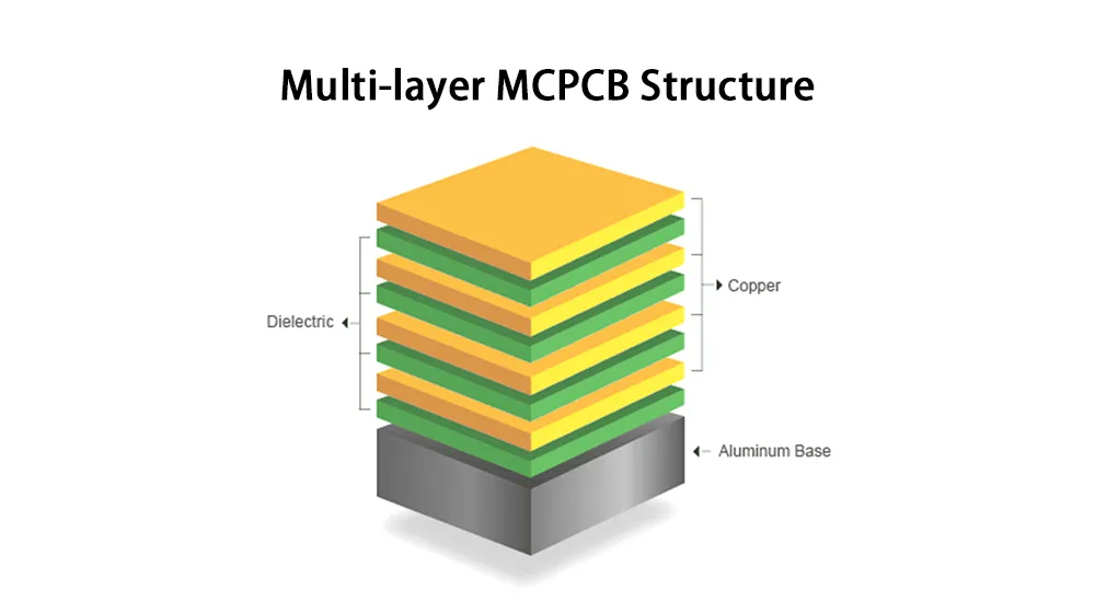
A two-layer MCPCB consists of a metal core and two copper conductive layers on the same side, with the metal base located at the bottom of the entire MCPCB. For complex designs, in a multilayer MCPCB, the layers will be evenly distributed on each side of the metal core. For instance, in a 12-layer board, the metal core will be at the center with 6 layers on the top and 6 layers at the bottom.
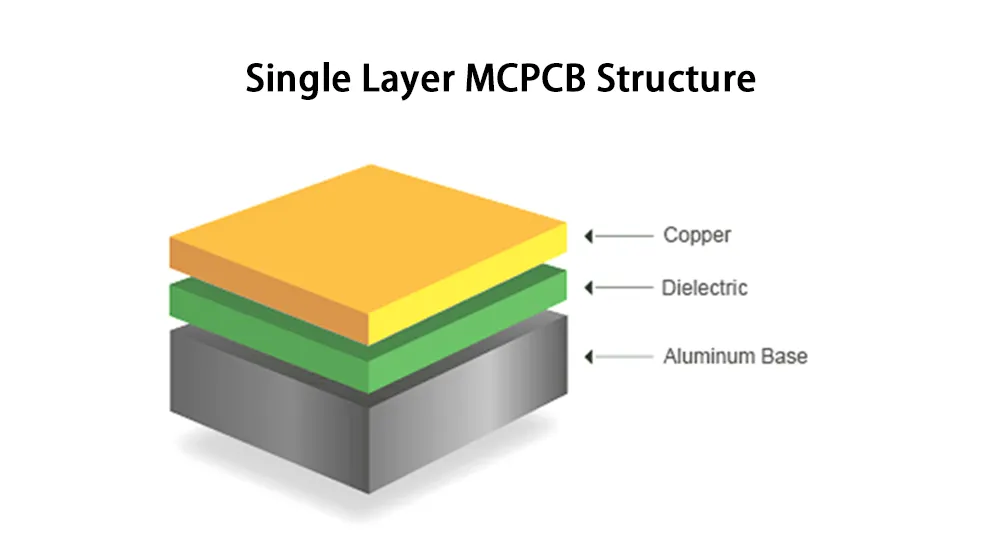
Single-Layer MCPCBs: Optimal for high-power LED applications, especially those using chip-on-board (COB) or surface-mounted LED packages, offering a direct and efficient thermal path from components to the metal core.
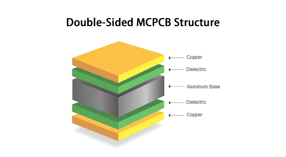
Double-Sided MCPCBs: Feature two layers of copper conductors with the metal core positioned between them, allowing conductor traces on both sides interconnected through vias.
Thermal Management Design Strategies
Component Placement Optimization
High-power components that generate significant amounts of heat should be placed near the center of the board, where the metal core can efficiently transfer heat away. Components especially sensitive to temperature should be placed in locations with the lowest temperature, such as the bottom of the board, keeping them away from components with high heat productivity.
Strategic Placement Guidelines:
- Position power semiconductors and high-current components directly above the metal core
- Maintain adequate spacing between heat-generating components to prevent hotspot formation
- Place temperature-sensitive analog components away from primary heat sources
- Consider thermal coupling effects between adjacent components
Thermal Via Implementation
Thermal vias play a crucial role in directing heat from component thermal pads to the metal core. You will likely need to include strategically placed thermal vias, a heat sink on each active component and power electronics, and active cooling measures near any other heat source on your circuit board.
Via Design Considerations:
- Via diameter: Larger vias provide better thermal conductivity
- Via density: Higher density improves heat transfer but may compromise routing
- Fill materials: Consider filled vias for improved thermal performance
- Placement: Position thermal vias as close as possible to heat-generating components
Copper Weight and Trace Design
Some manufacturers recommend using heavier copper (up to 10 oz) than would be used on FR4 to enhance thermal spreading. The copper layers act as thermal spreaders, distributing heat across the board surface before transferring to the metal core.
Manufacturing Process Considerations
Via Drilling and Plating Challenges
For multilayer dielectric stackups, the metal core must first be drilled to allow for layer transitions without creating a short circuit. First, slightly larger holes are drilled into the metal layer, and the holes are plugged with an insulating gel. This gel is cured and hardened, allowing it to be plated with copper, just like a standard via.
This creates difficulties in fabrication as a pre-drill/insulating filler/re-drill/plating process is used to form plated through holes. This process takes extra time and incurs extra costs, but is designed to prevent vias from shorting.
Manufacturing Process Flow:
- Initial drilling of oversized holes in metal core
- Insulating material filling and curing
- Secondary drilling to final via diameter
- Copper plating for electrical connectivity
- Quality inspection and testing
Design for Manufacturing (DFM) Guidelines
In the PCB layout, it’s best to apply an antipad to denote the region around the via hole that requires filling with insulating filler material. Be sure to size the via antipad so that IPC-2221 standards are followed.
Critical DFM Considerations:
- Minimum via sizes and aspect ratios for reliable plating
- Adequate clearances around metal core connections
- Surface finish selection for optimal thermal and electrical performance
- Solder mask color optimization (white for maximum heat reflection)
Electrical Design and Grounding Strategies
Metal Core Grounding Implementation
The core of the metal layer is grounded with the chassis ground or other ground to make it act as a shield for EMI issues during metal core PCB design. Connecting the metal core to the ground reduces ground loops and improves performance concerning signal stability.
Grounding Strategy Options:
- Heat Sink Configuration: Metal core acts as thermal spreader without electrical connection
- EMI Shield Configuration: Metal core connected to chassis or system ground
- Power Plane Integration: Metal core functions as low-impedance power distribution
When the board needs to be mounted near a high heat source, it is probably best not to ground the back side when connecting the top side to a standard power source; this will prevent ground loops.
High-Frequency Design Considerations
Usually, in high-frequency and high-speed circuits, the metal is used as a large ground plane. Metal core ground planes are capable of providing plane capacitance when there is a power-plane present in the board.
For high-speed applications, consider:
- Controlled impedance requirements with metal core presence
- Signal integrity analysis for critical nets
- EMI/EMC compliance with metal shielding effects
- Use of low-Dk, low-loss dielectric materials (such as ceramic-filled polyimide or alumina-based laminates)
- Power delivery network optimization
Application-Specific Design Optimization
LED Lighting Applications
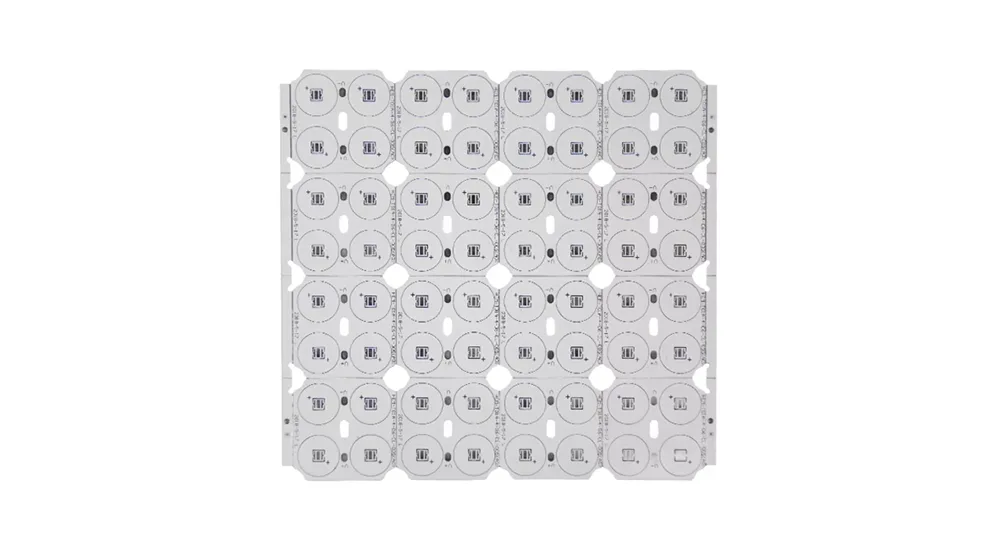
Single-layer PCBs ensure the lowest possible operating temperature and maximum brightness for LED bulbs and devices. LED applications benefit from:
- Direct thermal coupling between LED thermal pads and metal core
- Optimized copper spreading for uniform heat distribution
- White solder mask for enhanced light reflection
- COB (Chip-on-Board) integration capabilities
Power Electronics Implementation
High power systems can generate significant heat that needs quick removal to prevent component failure. Metal-core PCB design provides higher thermal conductivity to remove heat from important components.
Power electronics considerations include:
- High-current trace design with adequate copper weight
- Power component placement for optimal thermal management
- Isolation requirements for safety compliance
- Thermal cycling reliability under power fluctuations
Automotive and Aerospace Applications
Military and aerospace are two areas where printed circuit boards must withstand repeated thermal cycling, extremes of temperature and moisture, and frequent mechanical shocks. Metal core PCBs help satisfy these operational requirements as they provide greater structural integrity and thermal conductivity than boards built on FR4 laminates.
Quality Control and Testing Protocols
Thermal Performance Validation
Comprehensive testing ensures MCPCB designs meet thermal specifications:
- Thermal impedance measurements from junction to case
- Thermal cycling reliability testing
- Temperature mapping under operational conditions
- Thermal shock resistance evaluation
Electrical Testing Requirements
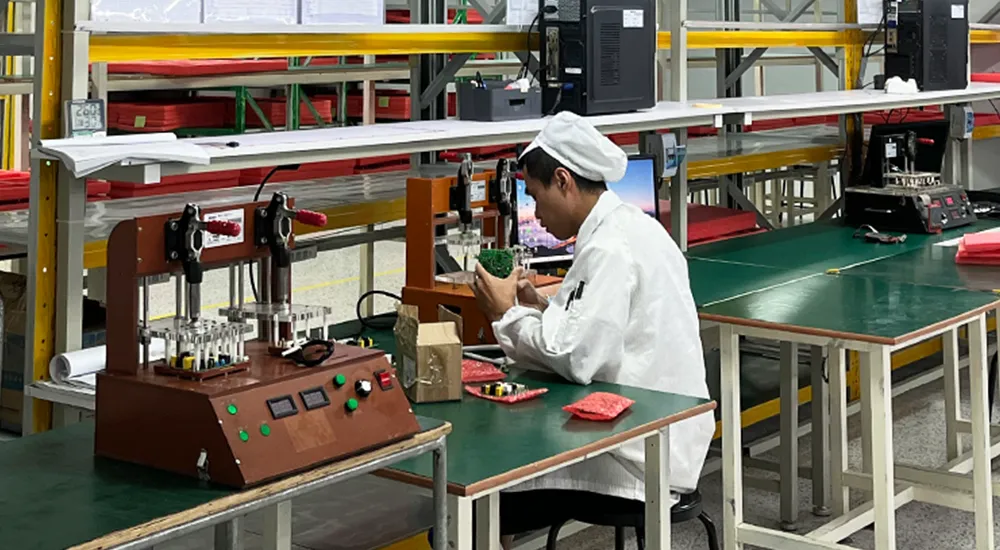
Conduct electrical and other functional tests to ensure circuit board quality, including in-circuit tests (ICT), functional tests (FCT), end-of-line testing (EOL), burn-in tests, and mechanical integrity checks.
Manufacturing Quality Metrics
Key quality indicators include:
- Via plating uniformity and adhesion
- Dielectric layer integrity and thermal conductivity
- Metal core flatness and surface finish quality
- Dimensional stability under thermal stress
Cost Optimization Strategies
Design Efficiency Improvements
Cost calculations should compare metal core designs with FR4 alternatives, carefully evaluating component costs, lead times, sourcing, and shipment expenses.
Cost Reduction Approaches:
- Panelization optimization for manufacturing efficiency
- Material selection balancing performance and cost
- Design standardization for volume advantages
- Supply chain optimization for material procurement
Manufacturing Process Optimization
V-cut depanelization processes for metal core PCBs should be designed during the design stage to maximize space utilization and reduce production costs.
Conclusion
Metal core PCB design demands thoughtful integration of thermal, electrical, and mechanical considerations. By leveraging the right materials, optimizing heat dissipation, and adhering to proven manufacturing practices, engineers can ensure both performance and reliability.
At Haoyue Electronics, we specialize in high-quality MCPCB solutions tailored for power electronics, LED lighting, and automotive systems. Need expert support for your next thermal-critical design? Contact us today for engineering consultation or a fast, tailored quote.
From prototype to production — we help hardware teams cut costs, improve yields, and scale faster. Let’s make your next product a success!

