Introduction
High speed PCB testing is essential for ensuring signal integrity and reliable performance in electronic systems operating from hundreds of MHz to several GHz. As digital designs push bandwidth limits, precise signal integrity test methods become critical.
Time Domain Reflectometry (TDR), Vector Network Analysis (VNA), and Eye Diagram testing are the core techniques for validating high-speed circuit performance, identifying impedance issues, and quantifying signal degradation. These methods help engineers verify design specifications, troubleshoot defects, and ensure compliance with high-frequency application standards.
Why High Speed PCB Testing is Critical
In high-speed digital systems, PCB traces behave as transmission lines rather than simple interconnections, making signal integrity testing essential. At multi-gigahertz frequencies, even small design or manufacturing variations can disrupt reliable operation.
Typical challenges include crosstalk between traces, impedance mismatches causing reflections, insertion loss reducing signal amplitude, and timing jitter degrading data quality. As edge rates become faster, these issues intensify and require precise testing to detect and control.
Without effective high speed PCB testing, signal integrity problems translate into higher error rates, narrower operating margins, and potential system failures. This makes dedicated methods such as TDR, VNA, and Eye Diagram indispensable for validating design performance.
TDR Testing for High Speed PCBs
Fundamentals of Time Domain Reflectometry
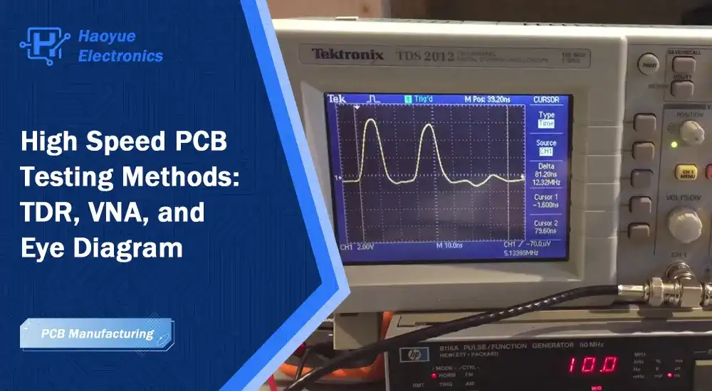
Time Domain Reflectometry (TDR) is one of the most effective methods for high speed PCB testing. It works by sending a fast rise-time signal into a trace and monitoring the reflections caused by impedance changes along the path. When the trace impedance deviates from the expected characteristic value, part of the signal is reflected back, revealing the location and severity of the discontinuity.
The reflection strength can be expressed by the coefficient ρ = (Z₂ – Z₁)/(Z₂ + Z₁), where Z₁ is the trace impedance and Z₂ is the point of discontinuity. This simple relationship allows engineers to quantify impedance mismatches with high precision.
Advanced TDR Analysis
TDR testing provides excellent spatial resolution, often down to millimeters, depending on the signal rise time. This makes it ideal for detecting defects such as via barrel variations, trace width inconsistencies, or dielectric thickness shifts that directly affect controlled impedance.
In addition to single-ended traces, differential TDR enables measurement of differential and common-mode impedance, as well as coupling effects. This is particularly valuable in high-speed serial interfaces like USB, HDMI, and PCIe, where differential signaling is standard.
Practical Implementation
Accurate TDR testing depends heavily on setup and calibration. Proper probe selection, calibration standards, and connection methods are crucial to avoid introducing additional errors. For multi-gigahertz applications, instruments typically require rise times below 35 ps to capture fine impedance details across the frequency range of interest.
When implemented correctly, TDR testing not only verifies design compliance but also helps identify subtle manufacturing issues before they impact product performance.
VNA (Vector Network Analyzer) for PCB Signal Analysis
A Vector Network Analyzer (VNA) characterizes high speed PCB performance in the frequency domain. By measuring S-parameters, VNA testing reveals how signals are transmitted, reflected, and attenuated across a wide frequency range, from DC up to millimeter-wave bands. This makes it an indispensable tool for understanding insertion loss, return loss, and phase behavior in complex PCB designs.
S-Parameter Fundamentals
S-parameters describe the relationship between input and output signals at each port of a circuit. In common two-port PCB tests:
- S₁₁ – input reflection, showing how much signal is reflected back due to impedance mismatch.
- S₂₁ – forward transmission, representing insertion loss or how much signal passes through.
- S₁₂ – reverse transmission, important in bidirectional paths.
- S₂₂ – output reflection, showing impedance match at the output port.
Together, these parameters quantify both transmission efficiency and reflection behavior. For example, insertion loss (|S₂₁|) highlights how trace length or dielectric material impacts attenuation, while return loss (|S₁₁|, |S₂₂|) indicates the quality of impedance matching. Phase data further enables calculation of group delay, revealing timing skew and dispersion that affect signal integrity.
Advanced VNA Techniques
Accurate high frequency PCB testing requires careful calibration. Methods like Short-Open-Load-Through (SOLT) compensate for fixture and cable effects, while time-domain gating helps isolate discontinuities within complex networks. These practices ensure that results reflect the PCB itself rather than the test setup.
For differential signaling, mixed-mode S-parameter measurements provide both differential and common-mode data. This allows engineers to evaluate mode conversion and common-mode rejection—key parameters for interfaces such as PCIe, HDMI, and USB that demand clean differential performance.

Eye Diagram
Eye Diagram Testing for Signal Integrity
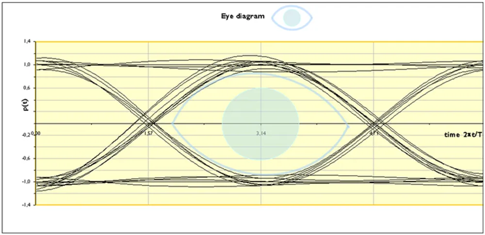
Eye diagram testing is one of the most intuitive ways to evaluate digital signal quality in high speed PCB design. By overlaying many bit periods of a waveform, the eye diagram creates a composite view that highlights timing relationships, noise effects, and signal degradation in a single display.
Eye Diagram Interpretation
The shape of the eye provides instant feedback on signal integrity:
- Eye height – amplitude margin, showing how much noise the system can tolerate.
- Eye width – timing margin, indicating the available window for correct sampling.
- Jitter – variations in edge timing, measured as peak-to-peak or RMS values.
- Crossing percentage – symmetry of the waveform, useful for detecting duty cycle distortion.
A wide, open eye suggests clean transmission, while eye closure signals degradation from jitter, intersymbol interference, or noise. These parameters directly correlate with bit error rate and system reliability.
Advanced Eye Diagram Analysis
Beyond visualization, eye diagrams support statistical analysis and compliance testing. Histogram analysis of voltage and timing distributions helps isolate noise sources and jitter components. Bathtub curve analysis further connects eye diagram data with predicted bit error rates, giving a quantitative view of system margins.
These advanced techniques are essential for validating compliance with standards such as PCIe, USB, and HDMI, and for ensuring long-term reliability in high speed digital systems.
Comparison of TDR, VNA, and Eye Diagram Methods
Each testing method addresses signal integrity from a different perspective. Choosing the right tool depends on the measurement goal, required accuracy, and application context.
Method Selection Criteria
| Testing Method | Purpose | Strengths | Limitations |
|---|---|---|---|
| Time Domain Reflectometry (TDR) | Measures impedance and detects discontinuities | High spatial resolution; fast fault detection | Less effective for complex frequency response |
| Vector Network Analysis (VNA) | Characterizes frequency-domain behavior (S-parameters) | Accurate; wide frequency coverage | Requires calibration; longer setup time |
| Eye Diagram Testing | Evaluates signal integrity and jitter | Visualizes timing and noise margin | Needs high-speed oscilloscope; interpretation required |
Complementary Testing Approaches
In practice, no single method is sufficient for complete high speed PCB testing. Engineers often combine all three:
- TDR – detect where impedance discontinuities occur.
- VNA – quantify how the PCB behaves across frequencies.
- Eye Diagram – confirm that real data streams meet timing and quality requirements.
By integrating these techniques, teams gain both root-cause insights and system-level assurance, ensuring robust design validation and reliable manufacturing outcomes.
Practical Considerations in High Speed PCB Testing
Test Environment and Setup
Accurate high speed PCB testing depends heavily on a controlled environment. External noise, ground loops, and thermal drift can distort results. Shielded setups, proper grounding, and temperature stabilization improve repeatability. Test fixtures must minimize parasitics while ensuring stable connections. Surface finishes also influence contact resistance and should be factored into test design.
Manufacturing Integration
In production, testing must balance coverage and throughput. Automated equipment supports high-volume screening with consistent accuracy. Applying statistical process control (SPC) to test data allows early detection of process shifts, reducing rework and improving yield.
Cost-Effectiveness Analysis
Each test method offers different cost-performance trade-offs. TDR provides a lower-cost option suitable for production checks. VNA delivers deeper frequency-domain insight, making it valuable for design validation despite higher instrument costs. The most efficient strategy aligns test precision with project needs and budget constraints.
Conclusion
TDR, VNA, and eye diagram testing each play a distinct role in high speed PCB validation. TDR is highly effective for locating impedance discontinuities, VNA enables full frequency-domain characterization, and eye diagram analysis provides direct visibility into digital signal quality. When combined, these methods form a complete toolkit for ensuring signal integrity in advanced electronic systems.
At Haoyue Electronics, we integrate these testing methodologies into our high speed PCB manufacturing and assembly processes. Our capabilities include:
- Comprehensive signal integrity testing – TDR, VNA, and eye diagram analysis for complete validation
- Impedance control assurance – precise design and verification for stable high-frequency performance
- Compliance with industry standards – ensuring reliable operation in demanding applications
- Prototype-to-production support – consistent testing practices across all manufacturing stages
If you are looking for a trusted partner with proven expertise in high speed PCB design, manufacturing, and testing, Haoyue Electronics can provide comprehensive solutions tailored to your application needs. Contact us today to discuss your project requirements and explore how we can help accelerate your development with robust, high-performance PCB solutions.
Frequently Asked Questions
What is the best method for signal integrity test in PCB design?
The best method depends on specific requirements and application context. TDR testing excels for impedance characterization and spatial resolution, VNA provides comprehensive frequency-domain analysis up to millimeter-wave frequencies, while eye diagram analysis offers direct assessment of digital signal quality. Most comprehensive validation strategies combine multiple techniques to address different aspects of signal integrity performance.
How to test signal integrity in high speed PCB during manufacturing?
Manufacturing-level signal integrity testing typically employs TDR measurements for impedance verification and basic connectivity testing due to speed and cost considerations. Automated TDR systems can rapidly verify characteristic impedance, identify shorts or opens, and detect major impedance discontinuities. For critical applications, selective VNA measurements may be performed on representative samples to ensure frequency-domain performance meets specifications.
Why is impedance testing important in PCB design for high-speed applications?
Impedance testing ensures proper signal transmission and minimizes reflections that can cause signal distortion, electromagnetic interference, and timing violations. In high-speed applications, impedance mismatches create standing wave patterns that degrade signal quality and reduce noise margins. Proper impedance control becomes increasingly critical as signal rise times decrease and operating frequencies increase, making accurate impedance testing essential for reliable system operation.

