Introduction
High speed PCB stackup design represents the foundation of successful multilayer PCB design in modern electronics. As signal frequencies exceed gigahertz ranges and edge rates become increasingly aggressive, proper stackup architecture directly influences signal integrity, electromagnetic interference control, impedance matching, and overall system performance.
The strategic arrangement of signal layers, power planes, and ground planes within a multilayer structure determines whether a high-speed design will meet its performance specifications while remaining cost-effective and manufacturable.
The Critical Role of Stackup in High-Speed Applications
High-Speed Circuits and Stackup Complexity
High-frequency circuits demand significantly more sophisticated stackup planning compared to traditional low-speed designs. Signal integrity becomes paramount when dealing with fast edge rates, where even minor impedance discontinuities can cause reflections, crosstalk, and timing violations. Unlike conventional circuits where stackup primarily affects cost and routing density, high-speed applications require careful consideration of electromagnetic field behavior, transmission line characteristics, and power delivery network performance.
Stackup and Signal Integrity
The relationship between stackup design and signal integrity in high-speed PCB applications extends beyond simple layer arrangement. Each conductor must maintain consistent impedance along its path, requiring precise control of trace geometry relative to reference planes. Power integrity also depends heavily on stackup configuration, as the power delivery network’s impedance profile directly impacts switching noise and power rail stability.
Stackup and EMI Control
EMI control represents another critical aspect where stackup design proves essential. Proper plane placement and layer symmetry help contain electromagnetic emissions while providing shielding against external interference. The fundamental difference between high-speed PCB design and standard PCB approaches lies in this holistic consideration of electrical performance rather than purely mechanical and routing concerns.

Common Multilayer Stackup Configurations
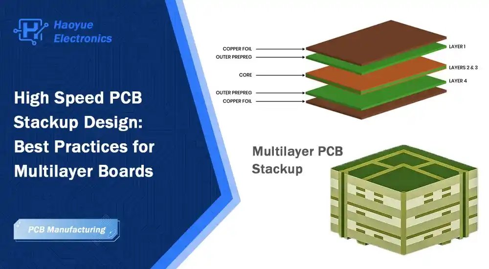
4-Layer Stackup for Entry-Level Applications
The basic four-layer configuration (Signal-Ground-Power-Signal) provides adequate performance for moderate-speed applications up to several hundred megahertz. This arrangement offers controlled impedance for surface traces while maintaining a dedicated ground plane for return current paths. However, the limited number of routing layers constrains design flexibility and may require careful via planning.
6-Layer PCB Stackup Design for Professional Applications
The 6 layer PCB stackup design represents the optimal balance between performance and cost for many high-speed applications. A typical configuration places signal layers adjacent to reference planes (Signal-Ground-Signal-Power-Ground-Signal), providing excellent controlled impedance environments for both single-ended and differential signals. This arrangement enables proper power plane decoupling while maintaining symmetrical construction to minimize warpage.
The middle signal layer, sandwiched between ground and power planes, offers exceptional electromagnetic containment and minimal crosstalk. This configuration particularly benefits differential pair routing, where consistent impedance and tight coupling prove essential for maintaining signal quality.
Advanced 8+ Layer Configurations
Complex applications such as high-speed servers, 5G infrastructure, and automotive radar systems often require eight or more layers. These stackups typically feature multiple power planes at different voltages, additional ground planes for enhanced shielding, and dedicated high-speed signal layers. The increased complexity allows for better power delivery network design, reduced electromagnetic interference, and improved thermal management.

Design Best Practices for Optimal Performance
Symmetrical Stackup Construction
A balanced stackup prevents board warpage and reliability issues. Uneven copper distribution causes thermal expansion mismatches, while symmetrical layer structures keep stress minimal during temperature changes.
Prepreg thickness also matters—uneven dielectric layers can offset symmetry. Work with your fabricator to ensure lamination processes maintain consistent thickness control.
Reference Plane Optimization
High-speed signals need continuous reference planes for stable impedance and low-inductance return paths. Keep power and ground planes tightly coupled (2–4 mils apart) to reduce PDN impedance and improve decoupling.
Microstrip routing (signal over plane) offers easier impedance control, while stripline (signal between planes) provides better shielding and lower crosstalk. Critical signals often benefit from stripline routing.
Material Selection Strategies
FR4 works for designs below ~1 GHz, but higher frequencies require low-loss dielectrics. Dielectric constant (Dk) and dissipation factor (Df) directly affect signal speed and attenuation.
Premium laminates such as Rogers, Megtron, or Panasonic R-5775 deliver superior performance but raise costs. Hybrid stackups—using FR4 for planes and low-loss materials for signal layers—offer a balanced solution.
Watch for glass weave effects that distort impedance on critical traces. Spread-glass or non-woven dielectrics solve this but at a higher price point.
Impedance Control and Via Management
Consistent impedance depends on trace geometry, dielectric thickness, and plane spacing. Common targets are 50 ohms for single-ended and 90–100 ohms for differential pairs.
Via design in high-speed PCB applications requires minimizing stub length and optimizing via size. Blind/buried vias or back-drilling reduce stub resonances but increase cost and complexity.

Real-World Application Examples
Communications Infrastructure
5G base stations and optical networking equipment demand exceptional signal integrity for multi-gigabit data rates. These applications typically employ 8-12 layer stackups with dedicated planes for different voltage domains and careful attention to power delivery network design. SerDes interfaces operating at 25+ Gbps require extremely low-loss materials and precise impedance control to maintain adequate signal margins.
Data Center and Server Applications
High-performance computing applications present unique challenges combining DDR memory interfaces, PCIe connections, and high-speed Ethernet. Memory interfaces require careful trace length matching and impedance control, while PCIe signals demand minimal crosstalk and excellent return loss performance. Eight-layer stackups commonly provide sufficient routing resources while maintaining controlled impedance for all critical signals.
Automotive Electronics
Advanced driver assistance systems and electric vehicle power modules operate in harsh electromagnetic environments while maintaining strict reliability requirements. Automotive radar applications at 77 GHz demand exceptional material stability and precise impedance control. Six to eight-layer stackups typically provide adequate performance while meeting automotive cost targets.
Practical Design Recommendations
Start stackup planning early and involve your PCB manufacturer from the concept stage. Feasibility checks on via sizes, lamination limits, and material options can prevent costly redesigns later.
Use simulation tools to validate stackup performance before prototyping. Field solvers help predict impedance shifts, crosstalk, and power delivery issues—saving time and reducing trial-and-error in hardware builds.
Balance performance with manufacturability. FR4 remains cost-effective and reliable for designs under ~1 GHz, while low-loss laminates should be chosen only when higher speeds truly demand them.
Conclusion
High-speed PCB stackup design is the foundation of successful multilayer PCB performance. A well-planned stackup ensures controlled impedance, reduces EMI, and delivers stable power distribution—while still meeting cost and manufacturing requirements.
As systems move to higher frequencies and tighter margins, mastering stackup design becomes critical. Engineers who apply these principles can achieve reliable, high-performance boards without repeated redesigns.
To achieve the best results, collaboration with an experienced PCB manufacturer is essential. Contact Haoyue Electronics to review your stackup needs and benefit from our expertise in high-speed design and advanced manufacturing solutions.
Haoyue Electronics: Professional High-Speed PCB Manufacturing Excellence
Successfully implementing complex high-speed stackup designs requires partnership with experienced manufacturers who understand both electrical requirements and manufacturing constraints. Haoyue Electronics specializes in advanced high-speed PCB design and manufacturing, offering comprehensive solutions from concept through production.
Our manufacturing capabilities include:
- Advanced stackup design consultation and electromagnetic simulation support
- Precision controlled impedance manufacturing with ±5% tolerance capability
- Low-loss material processing including Rogers, Isola, and Panasonic laminates
- Blind, buried, and microvias for complex interconnection requirements
- Comprehensive electrical testing including TDR impedance verification
- Assembly services with high-speed layout considerations for optimal performance
Our engineering team collaborates closely with customers during the design phase to optimize stackups for both electrical performance and manufacturing efficiency, ensuring first-pass success for critical high-speed applications.
Frequently Asked Questions
1. What is the best stackup for high speed PCB applications under 10 GHz?
For most high-speed applications under 10 GHz, a 6 layer PCB stackup design offers the optimal balance of performance and cost. The ideal configuration places high-speed signals on layers adjacent to reference planes (typically Signal-Ground-Signal-Power-Ground-Signal) to ensure controlled impedance and minimize electromagnetic interference. This arrangement provides excellent signal integrity PCB stackup performance while maintaining manufacturing feasibility with standard FR4 materials.
2. How do I choose between FR4 and low-loss materials for my high speed PCB stackup?
Material selection depends primarily on signal frequency and trace length requirements. FR4 materials work well for applications below 1-2 GHz with shorter trace lengths (under 6 inches). For higher frequencies or longer traces, PCB materials for high speed design such as Rogers RO4350B or Panasonic Megtron offer lower loss tangent (Df) and more stable dielectric constant (Dk), reducing signal attenuation and maintaining signal integrity over longer distances.
3. What stackup considerations are most critical for differential pairs?
Differential pair routing requires careful attention to impedance control and layer selection within the stackup. Place differential pairs on signal layers adjacent to solid reference planes to maintain consistent 90-100 ohm differential impedance. Avoid splitting differential pairs across multiple layers, and ensure adequate spacing from other high-speed signals to minimize crosstalk. The stripline configuration (signals between two reference planes) provides better electromagnetic containment than microstrip for critical differential signals.
4. How does stackup design affect power integrity in multilayer PCB design?
Power integrity depends heavily on the power delivery network formed by power and ground planes within the stackup. Adjacent power and ground planes should be separated by thin dielectrics (2-4 mils) to create low-impedance decoupling capacitance. Multiple power planes at different voltages require careful planning to avoid creating slots that can cause electromagnetic emissions. Proper power plane design within the stackup minimizes switching noise and maintains stable voltage delivery to high-speed circuits.
5. What manufacturing constraints should I consider when designing a high speed PCB stackup?
Key manufacturing constraints include minimum via drill sizes, lamination press capabilities, material availability, and impedance control tolerances. Blind and buried vias increase complexity and cost but may be necessary for dense designs. Aspect ratio limitations (board thickness to via drill diameter) typically constrain via sizes in thick stackups. Always consult with your PCB manufacturer early in the design process to ensure your proposed stackup is manufacturable within required tolerances and delivery schedules.

