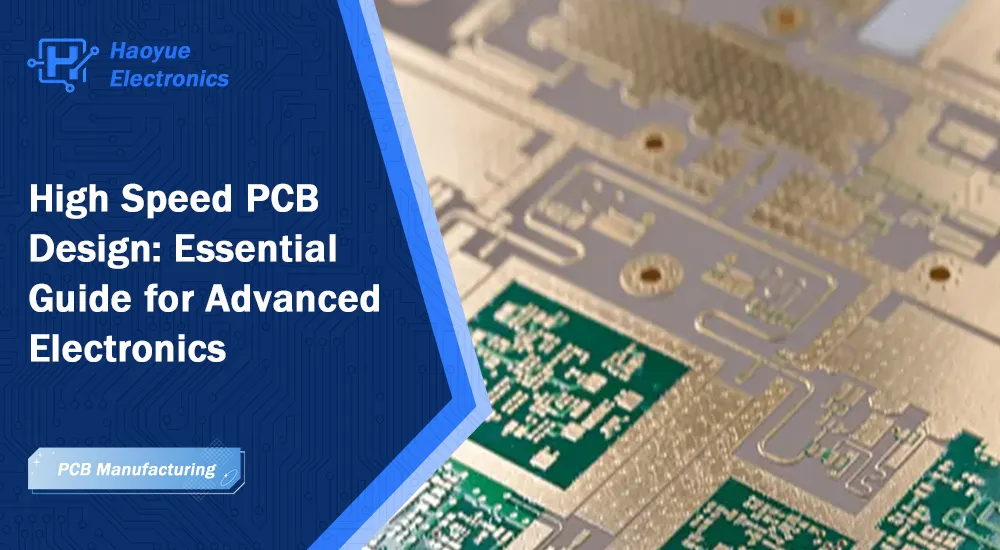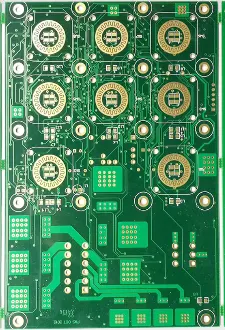
High speed PCBs are vital for 5G, AI servers, data centers, and automotive electronics. As circuits reach higher frequencies and data rates, mastering high speed design principles is key to signal integrity and system performance. This guide outlines the fundamentals of high speed PCB design, including definitions, critical parameters, materials, and manufacturing best practices.
What Defines a High Speed PCB
A high speed PCB is not defined by a fixed frequency threshold, but by the point where signal rise time becomes comparable to transmission line delay. When signals switch fast enough to be influenced by trace impedance, electromagnetic coupling, and propagation delay, traditional PCB design methods are no longer sufficient.
The key difference from standard PCBs lies in signal integrity requirements. While conventional boards operate without significant concern for electrical effects, high speed PCBs must carefully manage transmission line behavior, impedance control, EMI, and strict timing constraints.
Common Applications
High speed PCBs are widely used in advanced industries where fast, reliable data transfer is critical:
-
Telecommunications – 5G base stations, RF modules, and network infrastructure
-
Data Centers – server motherboards, storage systems, and high-speed interconnects
-
Automotive – advanced driver assistance systems (ADAS) and electric vehicle (EV) control units
-
Aerospace & Defense – radar systems, satellite communications, and mission-critical electronics
Core Design Challenge
The primary challenge is to preserve signal integrity while minimizing electromagnetic interference, power delivery noise, and thermal issues. Unlike designs focused solely on operating frequency, high speed PCB design requires simultaneous optimization of multiple electrical parameters across broad frequency ranges.
Critical Characteristics of High Speed PCB Design
High speed PCBs must balance multiple factors to ensure stable performance. The most important areas include signal integrity, impedance, power delivery, and EMI control.
Signal Integrity Management
Signal integrity is the foundation of high speed design. Poor management can cause data errors and timing failures.
-
Reflections – Caused by impedance mismatches; even 10% variation can create errors.
-
Crosstalk – Electromagnetic coupling between adjacent traces; reduced by proper spacing, routing, and ground plane use.
-
Timing – Issues such as clock skew, delay variations, and setup/hold violations require balanced trace lengths, controlled via usage, and careful routing topology.
Controlled Impedance Requirements
Consistent impedance ensures predictable signal transmission.
-
Targets – 50Ω single-ended and 100Ω differential are common.
-
Influencing factors – Trace width, dielectric thickness, copper weight, and stack-up.
-
Differential signaling – Provides better noise immunity by canceling common-mode interference; requires matched spacing, lengths, and optimized via design.
Power Integrity Considerations
Stable power delivery is essential for high speed systems.
-
Design methods – Decoupling capacitors, segmented power planes, and via stitching.
-
Target impedance – Must remain below 1Ω across DC to several GHz.
-
Optimization – Careful capacitor selection and power plane layout reduce inductance and resistance.
Electromagnetic Interference (EMI) Control
High speed PCBs are prone to EMI, requiring strong shielding and layout practices.
-
Ground planes – Provide return paths and isolation between layers.
-
Techniques – Ground stitching, optimized via placement, and separation of analog and digital circuits.
-
Effectiveness – Depends on plane continuity, via density, and keeping high speed traces close to reference planes.

Advanced Design Methodologies for High Speed PCBs
Design methodology directly affects signal quality, impedance control, and EMI performance. Key areas include stack-up, routing, via design, and grounding.
Stack-up Architecture
The stack-up defines both electrical and mechanical stability.
-
Layer arrangement – Place high speed signals near reference planes, minimize transitions, and keep symmetry for stability.
-
Power/ground planes – Provide stable return paths and support controlled impedance.
-
Dielectric selection – FR4 for moderate speeds; advanced materials (e.g., Rogers, Megtron) for GHz+ operation. Consistency ensures predictable electrical and thermal behavior.
Routing Methodologies
Proper routing reduces loss and timing issues.
-
Trace width/geometry – Calculated for impedance targets and manufacturing limits.
-
Length matching – Critical for clock/data signals; achieved with serpentine or meander routing.
-
Topology control – Balanced layouts help avoid skew and maintain signal quality.
Via Design Optimization
Vias directly impact high speed signal integrity.
-
Issues – Through-hole vias add parasitic inductance and capacitance.
-
Solutions
-
Shorten stub length to reduce reflections
-
Use blind/buried vias to minimize disruption
-
Apply via-in-pad for cleaner performance
-
Select proper via size for current and manufacturability
-
Grounding and Shielding Strategies
Ground and shielding are key to noise reduction.
-
Ground planes – Provide low-impedance return paths; continuity across layers is essential.
-
Techniques – Guard traces, ground stitching vias, and isolation of analog vs. digital circuits.
-
Shielding – Dedicated structures may be required for critical signals or sensitive analog sections.
Material Selection for High Speed Applications
The choice of materials directly affects signal integrity, power handling, and long-term reliability in high speed PCBs.
Advanced Substrate Materials
-
Rogers (RO4003C, RO4350B) – Low loss tangent, stable dielectric constant, excellent for GHz applications.
-
Panasonic Megtron (e.g., Megtron 6) – Combines low loss with high thermal conductivity, ideal for power-dense designs.
-
Isola (IS680, IS420) – Optimized for high speed digital and RF, with strong dielectric stability and low loss.
Dielectric Properties Impact
-
Dielectric constant (Dk) – Lower Dk = faster signal propagation; stability across frequency/temperature ensures consistent performance.
-
Loss tangent (Df) – Values below 0.01 are suitable for most high speed needs; ultra-low loss materials are used for very high frequency circuits.
Surface Finish Considerations
-
ENIG (Electroless Nickel Immersion Gold) – Flat, conductive, excellent for high frequency designs.
-
Immersion Silver – Lower insertion loss than HASL, good solderability.
-
OSP (Organic Solderability Preservative) – Cost-effective, suitable for short shelf-life products.
Testing and Verification Protocols
Testing ensures that high speed PCB designs meet performance and reliability targets. Key areas include signal integrity, power delivery, and thermal behavior.
Signal Integrity Verification
-
TDR (Time Domain Reflectometry) – Profiles impedance along traces, vias, and connectors to detect mismatches.
-
VNA (Vector Network Analyzer) – Uses S-parameters to measure insertion loss, return loss, and crosstalk.
-
Eye Diagram Analysis – Evaluates signal quality; eye opening shows timing margins, jitter reveals synchronization issues.
Power Integrity Assessment
-
Impedance Profiling – Confirms power distribution network stays below target impedance across DC–GHz ranges.
-
Noise Analysis – Identifies interference sources and validates decoupling/filtering.
-
Thermal Analysis – Uses thermal imaging and monitoring to detect hot spots, validate cooling strategies, and prevent reliability issues.
Future Developments in High Speed PCB Technology
Emerging Materials
-
Ultra-HDIs – Support finer features and higher layer densities.
-
Advanced dielectrics – Ultra-low loss materials enable mmWave operation.
-
Rigid-flex combos – Combine mechanical flexibility with high speed performance.
-
Embedded components – Reduce parasitics and improve density by integrating passives into substrates.
Manufacturing Evolution
-
Additive manufacturing – Enables 3D interconnects and rapid prototyping without traditional lithography.
-
Advanced metrology – Real-time inspection improves process control.
-
AI-driven optimization – Machine learning fine-tunes manufacturing parameters for better yield and performance.
Design Methodology Advancements
-
Co-design – Integrates mechanical, thermal, and electrical optimization for system-level performance.
-
Multi-physics simulation – Analyzes electromagnetic, thermal, and structural interactions.
-
AI-assisted design – Automatically generates routing solutions for complex constraints, ensuring manufacturability.
Conclusion
High speed PCB design is essential to next-generation electronics in telecom, computing, automotive, and aerospace. Success depends on mastering signal integrity, impedance control, power delivery, EMI management, and the right material choices.
As data rates climb, engineers who stay ahead with advanced design methods and emerging technologies will drive future innovation. Just as important, partnering with experienced manufacturers ensures that complex concepts become reliable, production-ready solutions.
High speed PCBs will remain the foundation of electronic systems that shape our technological future.
Haoyue Electronics: Advanced High Speed PCB Manufacturing Capabilities
Developing high speed PCBs requires expertise in materials, precision fabrication, and signal integrity. Haoyue Electronics delivers end-to-end solutions, from design support to mass production, helping customers bring complex projects to market quickly and reliably.
Core Capabilities
-
Design for Manufacturing (DFM) – Layout review and optimization for fabrication and assembly
-
Controlled Impedance – ±10% tolerance across multi-layer stack-ups
-
Advanced Via Technology – Blind, buried, and via-in-pad construction
-
Premium Materials – Rogers, Isola, Taconic, and other high-speed substrates
-
Rapid Prototyping – In-stock materials ensure short lead times
-
High Density Assembly – Fine-pitch BGAs, complex modules, and precise component placement
Quality & Support
Haoyue provides:
-
Comprehensive electrical testing and signal integrity validation
-
Strict process control to ensure reliability and consistency
-
Full turnkey service, from bare boards to final assembly and testing

