Introduction
Critical Role of High Frequency PCB Materials
As electronic systems advance into higher frequency domains, the selection of high-frequency PCB materials becomes increasingly critical for maintaining optimal performance.
Modern applications including 5G infrastructure, automotive radar systems, satellite communications, and emerging 6G technologies require advanced PCB materials that maintain signal integrity while minimizing losses at frequencies exceeding 20 GHz.
Impact of Material Selection on System Performance and Reliability
In high-frequency applications such as 5G and automotive radar systems, the selection of high-frequency PCB materials represents a critical decision that directly impacts system performance, manufacturing feasibility, and long-term reliability.
Challenges in High Frequency PCB Design
The evolution of high-frequency circuit board materials has transformed how engineers approach PCB design for demanding applications. High-frequency PCB materials must address unique electromagnetic challenges that become prominent as wavelengths approach circuit dimensions.
Unlike conventional PCB applications where mechanical properties and cost drive material selection, materials for high-frequency applications require sophisticated understanding of electromagnetic behavior and careful balance between electrical performance and practical manufacturing constraints.
Understanding High Frequency Design Challenges
Dielectric Losses and Signal Attenuation
The transition to high frequency design introduces multiple fundamental challenges, particularly above 1 GHz where dielectric losses become more significant than conductor losses, leading to primary signal attenuation.
Advanced PCB materials must address these challenges through carefully engineered properties that maintain performance stability. The skin effect confines current flow to increasingly thin layers near conductor surfaces, making surface roughness a critical factor that amplifies these losses.
Impedance Instability and Signal Integrity
Additionally, signal propagation speed varies inversely with frequency, and frequency-dependent dielectric constant changes can cause impedance instability, affecting signal integrity in broadband applications.
Temperature Stability and Performance Degradation
Temperature stability becomes paramount when selecting high-frequency materials because material properties experience significant variations with thermal cycling. Unlike low-frequency applications where minor property changes have negligible impact, high-frequency circuit board materials operating above 10 GHz can experience substantial performance degradation from small dielectric constant shifts.
These variations directly affect characteristic impedance, signal propagation delay, and insertion loss, making temperature-stable high frequency PCB materials essential for maintaining consistent performance across operating conditions.
Critical Material Properties for High Frequency Applications
Dielectric Constant and Loss Tangent Requirements
PCB material selection for high frequencies imposes strict requirements on materials, particularly regarding dielectric constant and loss tangent (Df) which significantly influence signal propagation speed and signal attenuation. For applications exceeding 10 GHz, ultra-low loss high-frequency materials become essential. Premium materials such as Rogers 5880 and Taconic TLY-5 feature exceptionally low loss tangent values that effectively minimize signal losses in demanding applications.
The dielectric constant determines signal propagation velocity and characteristic impedance in transmission line structures. Lower values enable faster signal propagation and reduced crosstalk, making these high-frequency materials valuable for high-speed digital applications. However, lower dielectric constants require wider trace geometries to achieve standard impedance values, potentially limiting circuit density in space-constrained designs.
Loss tangent directly determines power dissipation in dielectric materials, with power loss increasing proportionally with frequency and loss tangent. Materials for high-frequency applications must meet specific performance criteria based on their intended operating frequency range.
| Frequency Range | Recommended Df | Typical Applications |
|---|---|---|
| 1-5 GHz | < 0.005 | WiFi, Bluetooth, Sub-6 GHz 5G |
| 5-20 GHz | < 0.003 | mmWave 5G, WLAN, Radar |
| 20-40 GHz | < 0.002 | Automotive Radar, Satellite |
| > 40 GHz | < 0.0015 | High-resolution Radar, Test Equipment |
Thermal and Mechanical Stability
Glass transition temperature (Tg) serves as a fundamental material indicator that determines the upper operating temperature limit for reliable performance. Automotive and aerospace applications demand significantly stricter temperature stability requirements compared to consumer electronics, as these systems must maintain stable operation through frequent thermal cycling conditions. Materials must ensure consistent performance in environments where temperature excursions can reach extreme levels, such as engine compartments or high-altitude flight conditions.
Low z-axis coefficient of thermal expansion (CTE) materials effectively reduce mechanical stress induced by thermal cycling, minimizing risks of pad lifting or cracking. This becomes particularly critical in high-reliability applications where component failure could have severe consequences. The CTE mismatch between copper vias and substrate materials can induce mechanical stress leading to barrel cracking or pad lifting, making material selection crucial for long-term reliability in demanding environments.
Copper Foil and Surface Considerations
Copper surface roughness significantly impacts high frequency losses by amplifying the skin effect. Above 1 GHz, copper surface roughness intensifies the skin effect, increasing signal attenuation. Ultra-smooth copper foils with RMS roughness below 1 micron substantially reduce losses, making them ideal for high frequency applications.
Surface finish selection significantly impacts both high frequency electrical performance and assembly reliability. Common surface treatments include immersion silver (ImAg), organic solderability preservative (OSP), and electroless nickel immersion gold (ENIG), each offering distinct advantages and disadvantages for different application scenarios. The choice depends on balancing electrical performance requirements against assembly reliability and cost considerations.
Material Categories and Selection Guidelines
Advanced FR4 Formulations
Modern low-loss FR4 materials represent significant improvements over standard epoxy-glass formulations, incorporating specialized resin systems and glass weave patterns to achieve enhanced high frequency performance. These advanced PCB materials typically achieve loss tangent values between 0.002 and 0.004 at 10 GHz while maintaining processing familiarity and cost advantages of traditional FR4 systems.
The glass weave pattern requires careful consideration in high frequency PCB materials, as periodic variations in glass fiber density can create local impedance variations that manifest as insertion loss ripple in the frequency domain. Flattened glass weave patterns or spread glass constructions help minimize these effects while maintaining mechanical strength requirements essential for reliable manufacturing.
PTFE-Based High Performance Materials
PTFE-based high performance materials offer significant advantages through extremely low loss tangent (Df) values and stable dielectric constants, making them exceptional choices among high-frequency circuit board materials. However, PTFE’s low surface energy creates weak copper adhesion, requiring specialized surface treatments or bonding agents to ensure long-term reliability. Despite these manufacturing challenges, PTFE materials deliver outstanding performance in aerospace, radar, and other high-demand environments where electrical performance takes priority over processing complexity.
The inherent chemical inertness of PTFE provides excellent long-term stability and moisture resistance, particularly valuable in harsh environmental applications. Processing these high-frequency materials requires specialized fabrication techniques including controlled thermal cycles and modified drilling parameters. The coefficient of thermal expansion mismatch between PTFE and copper necessitates careful via design and potentially alternative interconnection strategies for the most demanding applications.
Ceramic-Filled Composite Materials
Ceramic-filled laminates offer tailored electrical properties through controlled addition of ceramic particles to polymer matrices. These materials enable precise dielectric constant adjustment while potentially improving thermal conductivity and dimensional stability compared to unfilled polymer systems. The ceramic loading level directly influences both electrical and mechanical properties, with higher loading typically providing higher dielectric constant and improved thermal performance.
Frequency-Specific Material Selection
Sub-6 GHz Applications
For frequencies below 6 GHz, PCB material selection for high frequencies focuses on achieving adequate performance while maintaining cost effectiveness and manufacturing simplicity. Standard low-loss FR4 materials often provide sufficient performance for these applications, particularly when combined with appropriate copper foil selection and surface finish optimization tailored for high-frequency applications.
Recommended high frequency PCB materials for this frequency range include Rogers RO4350B with Dk=3.48 and Df=0.0037 at 10 GHz offering excellent processability, Isola I-Tera MT40 featuring Dk=3.45 and Df=0.0031 at 10 GHz with low-loss glass weave construction, and Panasonic Megtron 6 providing Dk=3.4 and Df=0.002 at 5 GHz with automotive qualification credentials.
mmWave and Ultra-High Frequency Systems
Applications operating above 20 GHz require premium high-frequency circuit board materials with exceptional electrical performance characteristics. At these frequencies, even small material imperfections can significantly impact system performance, making material uniformity and surface quality critical selection criteria for high frequency PCB materials. Ultra-low loss tangent becomes essential, as insertion losses increase dramatically with frequency.
Premium material options for extreme frequency applications include Rogers RT/duroid 5880 offering Dk=2.2 and Df=0.0009 at 10 GHz in PTFE ceramic composite formulation, Taconic TLY-5 providing Dk=2.2 and Df=0.0009 at 10 GHz with woven glass reinforcement, and Rogers RO3003 featuring Dk=3.0 and Df=0.0013 at 10 GHz in ceramic-filled PTFE construction.
Hybrid Stackup Strategies
Hybrid stackups combine different high-frequency materials within a single PCB to optimize performance while controlling costs. This approach typically places high-performance materials on signal layers carrying critical RF signals while using standard materials for power distribution and ground planes. The design of transitions between different materials for high-frequency applications requires careful attention to impedance matching and thermal expansion compatibility.
Design and Manufacturing Considerations
Via Technology Optimization
Via design becomes increasingly critical as frequencies rise and wavelengths shrink. Standard through-hole vias create parasitic inductances and capacitances that can significantly impact circuit performance, particularly in multilayer designs where via stubs extend beyond signal routing layers. Back-drilling technology removes unused via stubs to eliminate resonances that can create significant insertion loss peaks at specific frequencies.
Critical via design parameters include:
- Diameter: Minimize to reduce parasitic inductance while maintaining manufacturability
- Aspect Ratio: Maintain below 8:1 for reliable plating and consistent impedance
- Back-drilling: Essential for frequencies above 10 GHz to eliminate stub resonances
- Microvias: Enable controlled impedance transitions with minimal parasitic effects
Process Control and Quality Assurance
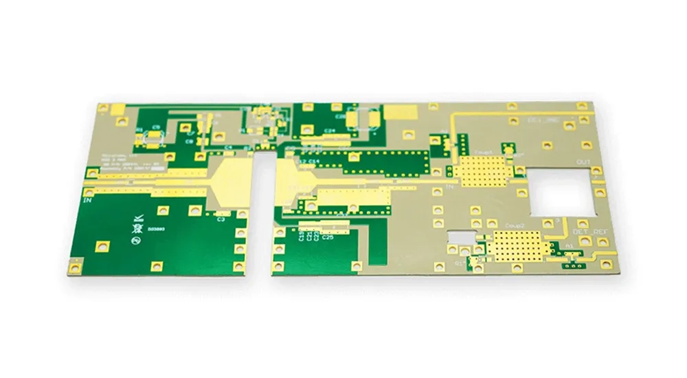
High frequency PCB manufacturing demands stringent process control to maintain tight tolerances necessary for consistent electrical performance. Common manufacturing challenges include material thickness variations that directly impact impedance control, and copper thickness inconsistencies that affect insertion loss and crosstalk characteristics. These issues become particularly problematic in high frequency applications where even minor variations can significantly degrade performance.
Using Time Domain Reflectometry (TDR) and Vector Network Analyzers (VNA) for testing helps comprehensively evaluate insertion loss, return loss, and crosstalk performance, ensuring each board’s electrical characteristics meet design requirements. Advanced process monitoring and statistical process control become essential for achieving the repeatability required in high frequency applications, with quality assurance protocols including both electrical and mechanical testing under conditions representative of actual operating environments.
Testing and Validation Methodologies
Material Characterization
Accurate measurement of material properties is essential for reliable high frequency design. The Split Post Dielectric Resonator (SPDR) method provides the most accurate measurement of dielectric constant and loss tangent but requires specialized test fixtures and calibration procedures. Stripline resonator methods offer practical measurement techniques that better represent actual circuit conditions but may be influenced by processing variations and copper roughness effects.
Performance Validation
Comprehensive validation of high frequency PCB materials requires both electrical and reliability testing under conditions representative of actual operating environments. S-parameter measurements across the full operating frequency range provide quantitative assessment of insertion loss, return loss, and crosstalk performance. Thermal cycling tests verify material stability and mechanical reliability under temperature excursions typical of operating conditions.
Cost-Performance Optimization
The selection of high frequency PCB materials requires careful balance between performance requirements and economic constraints. Premium high-frequency materials may provide superior electrical performance but often come with significantly higher costs and processing complexity that can impact overall project economics. A systematic approach to cost optimization involves identifying specific performance requirements for each circuit function and selecting materials for high-frequency applications accordingly.
Volume production considerations significantly impact material selection for high-frequency applications, as high-volume applications may justify qualification costs for premium high frequency PCB materials while low-volume applications may require selection from readily available standard materials. Long-term supply chain stability and second-source availability become important factors for products with extended life cycles requiring consistent access to specialized high-frequency circuit board materials.
Future Technology Trends
The high frequency PCB materials industry continues evolving in response to advancing application requirements and emerging technologies. Ultra-low loss materials with loss tangent values below 0.0005 are being developed for the most demanding applications while maintaining acceptable mechanical properties and processing characteristics. These next-generation high-frequency materials promise to enable even more challenging applications in 6G communications and advanced radar systems.
Thermoplastic materials offer potential advantages in terms of recyclability and processing flexibility for high-frequency applications, though current electrical properties limit their application to less demanding frequency ranges. Nanotechnology approaches to material enhancement offer possibilities for tailoring properties at the molecular level, potentially enabling high frequency PCB materials with unprecedented combinations of electrical, thermal, and mechanical properties. However, these technologies remain primarily in development stages and require significant additional work before commercial availability in high-frequency circuit board materials.

Expert Partnership in High Frequency PCB Manufacturing
Successful implementation of high frequency PCB designs requires a comprehensive understanding of the complex interactions between material properties, design requirements, and manufacturing processes. The most successful projects result from close collaboration between design teams and experienced manufacturing partners who can translate theoretical material properties into practical, manufacturable solutions using appropriate high frequency PCB materials.
Haoyue Electronics Expertise
Haoyue Electronics specializes in high frequency PCB manufacturing and assembly, with extensive experience across the complete spectrum of advanced PCB materials and processing technologies. Our engineering team combines deep technical expertise with practical manufacturing knowledge to help optimize PCB material selection for high frequencies based on specific application requirements while ensuring reliable, cost-effective production.
Comprehensive Capabilities
- Material Characterization: Ensuring precise material properties to meet the needs of high frequency designs.
- Design Validation: Thorough testing to validate performance and functionality before full-scale production.
- Full Production Services: Providing end-to-end production support, from prototyping to mass production.
Our expertise spans a range of high-frequency applications, including:
- 5G Infrastructure
- Automotive Radar
- Aerospace Systems
Seamless Transition from Prototyping to Volume Production
We maintain qualified processes for the full range of high-frequency circuit board materials and surface finishes, enabling rapid prototyping and seamless transition to volume production. Whether you are developing next-generation wireless communication systems, advanced radar applications, or precision test equipment, our expertise in materials for high-frequency applications and manufacturing processes ensures that your designs achieve optimal performance while meeting cost and schedule objectives.
Contact us today to discuss your high frequency PCB needs and how Haoyue Electronics can help bring your project to life with precision and reliability.

