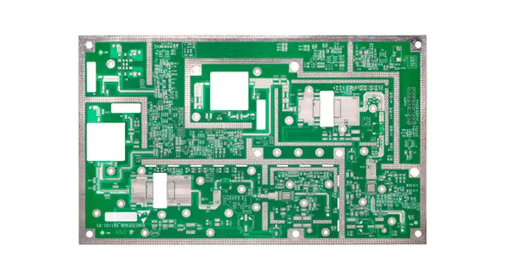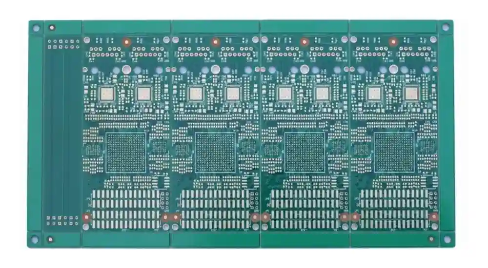
High frequency PCB design has become increasingly crucial as modern electronic systems push the limits of signal transmission speeds and operating frequencies. A PCB operating at frequencies of 100 MHz or higher is considered a high frequency PCB, with some designs extending into the gigahertz range for applications like 5G communications, radar systems, and aerospace equipment.
Understanding the core principles and challenges of high frequency PCB design is essential for engineers working on next-generation electronic systems that require superior performance and signal integrity. The transition from standard PCB design to high frequency applications introduces complex electromagnetic phenomena that require specialized strategies.
At high frequencies, PCB traces function as transmission lines with distinct impedance characteristics at each point along their path, making signal integrity a critical concern. This shift demands careful attention to factors such as material selection, precise impedance control, effective electromagnetic interference (EMI) management, and manufacturing accuracy to ensure reliable performance in high-speed electronic circuits.
Material Selection for High Frequency Applications
Advanced Substrate Materials
The foundation of successful high frequency PCB design lies in selecting the right substrate materials that maintain signal integrity at elevated frequencies. Conventional FR-4 substrates, while cost-effective for standard applications, have significant limitations in high frequency environments. These limitations include increased dielectric losses, inconsistent dielectric constants, and poor thermal stability, which can compromise performance at higher frequencies.
Materials from Rogers Corporation have emerged as industry standards for high frequency applications, offering specialized PTFE-based and hydrocarbon ceramic composite laminates engineered for optimal performance across MHz to GHz frequency ranges. The Rogers 4000 series, particularly RO4350B, features a dielectric constant of 3.48 and exceptional thermal stability, making it ideal for power amplifiers and RF circuits that operate up to 40 GHz.
Material Property Comparison
| Material Type | Dielectric Constant (Dk) | Loss Tangent (Df) | Applications | Frequency Range |
|---|---|---|---|---|
| Standard FR-4 | 4.5 | 0.020 | General purpose | Up to 1 GHz |
| Rogers RO4350B | 3.48 | 0.0037 | RF/Microwave | Up to 40 GHz |
| Rogers RT/duroid 5880 | 2.20 | 0.0009 | mmWave antennas | Up to 77 GHz |
| PTFE (Teflon) | 2.1-2.55 | 0.0002 | Ultra-high frequency | Above 100 GHz |
PTFE and Ceramic-Filled Materials
PTFE-based materials offer superior electrical performance with lower signal loss, excellent thermal stability, and chemical resistance, making them preferred choices for radio frequency applications. These materials can be enhanced with ceramic fillers to achieve specific dielectric properties while maintaining mechanical stability. Ceramic fillers lower the material’s dielectric constant and dissipation factor, minimizing signal losses crucial for maintaining signal strength in RF applications.
The selection process requires careful evaluation of operating frequency ranges, environmental conditions, and cost considerations. Above approximately 5-10 GHz, FR4 materials experience excessive dielectric losses, making Rogers materials an industry standard for rigid microwave and RF PCBs.
Signal Integrity and Impedance Control
Controlled Impedance Design
Controlled impedance refers to the characteristic impedance of transmission lines formed by PCB traces and their associated reference planes. This is essential for high-speed signal propagation without distortion. As signal frequencies increase, impedance control becomes even more critical, as even minor impedance variations can cause significant signal reflections and degradation.
Impedance control requires precise management of trace geometry, dielectric properties, and layer stack-up configuration to maintain consistent impedance values throughout the signal path. Key parameters include trace width and thickness, the dielectric constant of substrate materials, and the distance to reference planes.
Trace Routing and Geometry
Effective high frequency PCB layout demands careful attention to trace routing techniques. Traces should be kept as short and direct as possible, with curved transitions preferred over sharp corners to minimize impedance discontinuities and signal reflections. The 3W rule for spacing between traces becomes even more critical at high frequencies, with minimum spacing increasing to 5W for high frequency signals and up to 50 mils for periodic signals, such as clocks, to achieve better isolation.
Via Management and Return Paths
In high frequency PCB routing, fewer vias are preferred as each via introduces approximately 0.5 pF of distributed capacitance, potentially degrading signal speed and introducing data errors. Via stubs create impedance discontinuities that can severely impact signal integrity, requiring careful consideration of via placement and the use of blind and buried vias in complex multilayer designs.
High frequency signals require well-defined return paths, typically through solid ground planes. Interrupted return paths can cause unwanted noise and radiation. Continuous reference planes are essential for maintaining controlled impedance and providing low-impedance paths for return currents.

EMI Management and Shielding Techniques
Electromagnetic Interference Challenges
High frequency and high-speed boards often include components that radiate EMI emissions, such as wireless transmitters, converters, and power supplies. These devices generate onboard interference that can distort the electromagnetic compatibility of the surrounding environment. The challenges become more pronounced as frequencies increase, with even minor design oversights potentially causing significant interference issues.
Grounding and Shielding Strategies
Effective PCB EMI shielding requires a systematic approach that takes into account ground planes, shielding layers, component placement, impedance control, and filter capacitors. A continuous ground plane serves multiple functions: providing a stable reference voltage, minimizing EMI through absorption and redirection of electromagnetic energy, and creating low-impedance return paths for high frequency currents.
Advanced Shielding Techniques
Modern high frequency PCB designs often incorporate specialized shielding approaches:
- Via Fencing: Strategic placement of grounded vias around sensitive circuits to create electromagnetic barriers
- Guard Traces: Grounded traces positioned between sensitive signal paths to reduce crosstalk
- Copper Pour Shielding: Large copper areas connected to ground planes to provide localized shielding
- Component-Level Shielding: Integration of shield cans or conductive coatings for critical circuit sections
Materials with stable dielectric properties and low loss help maintain signal integrity at high frequencies, with conductive coatings enhancing shielding effectiveness when properly implemented.
Design Guidelines and Manufacturing Considerations
Layer Stack-up Design
High-speed designs require specific stackup layers to help with EMI shielding and signal integrity, with the primary consideration being full and continuous reference planes on internal layers. The stack-up design must balance signal integrity requirements with manufacturing constraints and cost considerations.
Multi-layer configurations typically include dedicated power and ground planes, with signal layers positioned to minimize crosstalk and maintain consistent impedance. Microstrip and stripline configurations are commonly used to control impedance and reduce radiation from high frequency signals.
Manufacturing Precision Requirements
High frequency PCBs require incredibly accurate manufacturing to maintain consistent electrical properties, with tight manufacturing tolerances essential for achieving specified performance. Critical manufacturing considerations include:
- Copper Foil Selection: Ultra-smooth copper foils reduce skin effect losses at high frequencies
- Dielectric Thickness Control: Precise control of dielectric thickness to maintain impedance specifications
- Registration Accuracy: Tight layer-to-layer registration to ensure consistent trace positioning
- Surface Finish: Appropriate surface finishes that maintain signal integrity while ensuring reliable soldering
Design Verification and Testing
Testing and measuring impedance using tools like Time-Domain Reflectometry (TDR) or Vector Network Analyzers (VNA) is essential to verify that the PCB design meets specified impedance requirements. Advanced simulation tools enable engineers to model signal behavior and identify potential issues before fabrication, significantly reducing development time and costs.

Conclusion
High frequency PCB design represents a sophisticated engineering discipline requiring a deep understanding of electromagnetic principles, advanced materials, and precision manufacturing techniques. Success demands careful integration of material selection, impedance control, EMI management, and design verification throughout the development process.
The rapid advancement of technologies such as 5G communications, automotive radar, and IoT devices continues to drive demand for higher frequency capabilities and more sophisticated PCB designs. Engineers must stay current with evolving materials, design techniques, and manufacturing capabilities to meet these challenging requirements.
Partner with Haoyue Electronics for Your High Frequency PCB Needs
At Haoyue Electronics, we understand the critical importance of precision and expertise in high frequency PCB manufacturing and assembly. Our advanced facility specializes in handling complex RF and microwave designs, featuring state-of-the-art equipment capable of maintaining the tight tolerances required for optimal high frequency performance.
Our experienced engineering team works closely with clients to optimize designs for manufacturability while ensuring signal integrity specifications are met. From material selection guidance to design rule verification, we provide comprehensive support throughout your project lifecycle. With capabilities spanning Rogers materials, PTFE substrates, and ceramic-filled composites, we deliver reliable solutions for aerospace, telecommunications, medical, and advanced communication applications.
Contact Haoyue Electronics today to discuss how our expertise in high frequency PCB manufacturing and assembly can support your next-generation electronic designs.
FAQ
1. What is High Frequency PCB Design?
High frequency PCB design refers to the design and manufacturing process of printed circuit boards (PCBs) that operate at frequencies above 100 MHz, typically used in applications like 5G communications, RF/microwave circuits, and aerospace systems. These PCBs must maintain signal integrity and manage electromagnetic interference (EMI) to ensure optimal performance at high speeds and frequencies.
2. What materials are best for High Frequency PCBs?
The best materials for high frequency PCBs include specialized substrates like Rogers RO4350B and PTFE-based laminates. These materials offer low dielectric losses and stable performance at high frequencies. Rogers materials, in particular, are widely used in RF and microwave applications due to their excellent thermal stability and minimal signal loss.
3. Why is Impedance Control important in High Frequency PCB Design?
Impedance control is crucial for maintaining signal integrity in high frequency PCB designs. As signal frequencies increase, even small variations in impedance can lead to signal reflections and degradation. Effective impedance control involves precise management of trace geometry, dielectric properties, and layer configurations to ensure consistent impedance values along the signal path.
4. How can EMI be minimized in High Frequency PCB Designs?
Electromagnetic Interference (EMI) can be minimized by using grounding and shielding strategies. These include employing continuous ground planes, incorporating via fencing and guard traces, and utilizing copper pour shielding. Properly implemented shielding can absorb and redirect electromagnetic energy, minimizing signal degradation and ensuring optimal performance.
5. What are the key manufacturing requirements for High Frequency PCBs?
Manufacturing high frequency PCBs requires precise control over several factors, including copper foil selection, dielectric thickness, registration accuracy, and surface finishes. High frequency designs demand tight tolerances to ensure consistent electrical properties and maintain signal integrity throughout the board. These precision requirements are essential for achieving the specified performance in high-speed and high frequency applications.

