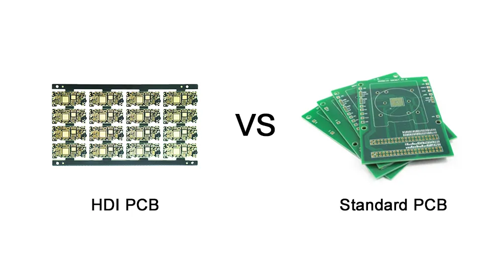
This technical comparison examines six fundamental differences between HDI and standard PCB technologies, providing engineers with essential information for informed technology selection decisions.
1. Size and Weight: The Miniaturization Advantage
HDI PCBs deliver dramatic size and weight reductions compared to standard PCB designs through build-up multilayer construction. While standard PCBs rely on traditional double-sided or simple multilayer approaches, HDI technology uses sequential lamination of thin layers onto a core substrate.
This construction method enables HDI boards to achieve the “light, thin, short, and small” characteristics essential for modern portable devices. Standard PCBs cannot match these dimensional advantages due to their reliance on thicker materials and simpler layer structures. The result is HDI boards that occupy up to 60% less space while maintaining equivalent or superior functionality.
2. Layer Count and Routing Density: Beyond Traditional Limits
Standard PCBs typically utilize 2-4 layers, limiting routing flexibility and component placement options. HDI PCBs commonly incorporate 6-12 layers or more, with some advanced applications requiring even higher layer counts to support complex circuit requirements.
This increased layer capacity directly translates to superior wiring density. HDI designs achieve line widths and spacing of 76.2 micrometers or less, compared to the broader traces required in standard PCB manufacturing. The pad density in HDI configurations exceeds 50 joints per square centimeter, enabling component miniaturization that standard PCBs cannot accommodate.
3. Via Technology: Precision Beyond Mechanical Drilling
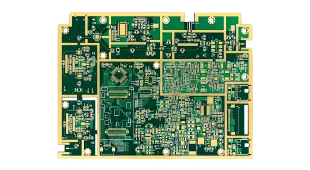
The most significant technical distinction lies in via formation and implementation. Standard PCBs rely exclusively on mechanically drilled through-hole vias, limiting design flexibility and increasing board real estate consumption.
HDI PCBs employ three distinct via types: through-hole, blind, and buried vias. Blind vias connect outer layers to internal layers without penetrating the entire board thickness. Buried vias provide connections between internal layers while remaining completely enclosed within the board structure. These micro-vias, created through laser drilling technology, achieve diameters less than 150 micrometers with precision impossible through mechanical drilling methods.
4. Electrical Performance: Superior Signal Integrity
HDI technology delivers measurably superior electrical performance through multiple engineering advantages. The increased interconnect density enables shorter signal paths, reducing transmission delays and improving overall system response times. Controlled impedance characteristics become more predictable with HDI stack-up configurations, supporting high-frequency applications and digital signal processing requirements.
Standard PCBs cannot match HDI performance in electromagnetic interference suppression, radio frequency interference mitigation, or static discharge protection. The additional layer capacity in HDI designs enables more effective ground plane implementation and superior thermal management through enhanced thermal conduction paths.
5. Manufacturing Complexity: Advanced Process Requirements
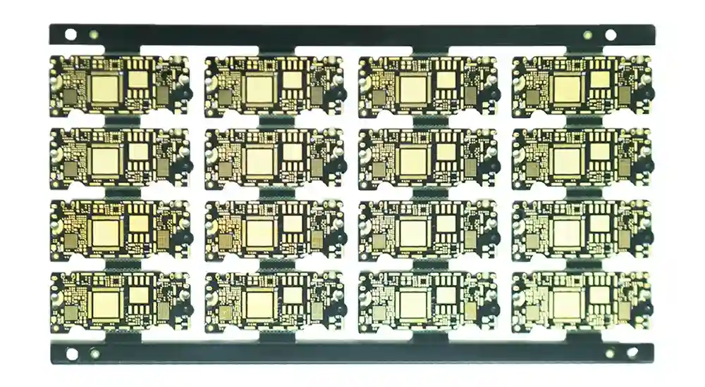
HDI PCB manufacturing requires significantly more sophisticated processes compared to standard PCB production. The sequential build-up manufacturing process demands precise temperature and pressure control during multiple lamination cycles, with laser drilling technology replacing mechanical drilling for via formation.
Standard PCB manufacturing utilizes established mechanical drilling and conventional lamination processes that require less specialized equipment and expertise. HDI production demands specialized laser drilling systems, precision lamination equipment, and advanced plating technologies that represent substantial capital investments.
The critical challenge in HDI manufacturing involves buried via plugging processes. Inadequate via filling results in surface irregularities, thickness variations, and pad defects that compromise board functionality. Standard PCBs avoid these complex process requirements entirely.
6. Cost Structure: Investment vs Performance Returns
HDI PCBs typically involve higher initial manufacturing costs due to advanced equipment requirements, specialized materials, and increased process complexity. The technology demands highly skilled technicians and engineers, increasing labor costs compared to standard PCB production.
However, HDI technology often provides superior value in applications requiring miniaturization, enhanced performance, or reduced system complexity. The ability to integrate more functionality into smaller form factors can reduce overall system costs by eliminating multiple boards or external components. High-volume production helps amortize the additional tooling and setup costs, making HDI increasingly cost-effective for consumer electronics applications.
Standard PCBs maintain cost advantages for simple circuits with relaxed size constraints and conventional performance requirements.
Comprehensive Comparison Summary
The following table provides a direct comparison of the key characteristics that distinguish HDI PCB from standard PCB technology:
| Feature | HDI PCB | Standard PCB |
|---|---|---|
| Layer Count | 6-12+ layers typical | 2-4 layers typical |
| Board Thickness | Thinner profile with 80μm dielectric | Thicker profile with standard dielectric |
| Via Types | Through-hole, blind, buried vias | Primarily through-hole vias only |
| Via Size | <150μm (laser drilled) | >200μm (mechanically drilled) |
| Line Width/Spacing | ≤76.2μm | >100μm typically |
| Pad Density | >50 joints/cm² | <30 joints/cm² |
| Drilling Method | Precision laser drilling | Mechanical drilling |
| Weight | Significantly lighter | Heavier due to thickness |
| Signal Integrity | Superior high-frequency performance | Standard performance |
| EMI/RFI Suppression | Enhanced shielding capability | Basic shielding |
| Manufacturing Complexity | High precision, sequential build-up | Conventional processes |
| Equipment Requirements | Specialized laser and lamination systems | Standard PCB equipment |
| Initial Cost | Higher investment | Lower initial cost |
| Applications | Mobile devices, aerospace, medical | Consumer electronics, industrial |
| Production Volume | Cost-effective at high volumes | Suitable for all volumes |
Conclusion
The choice between HDI PCB and standard PCB technology depends fundamentally on application requirements, performance specifications, and cost targets. HDI technology provides superior miniaturization, enhanced electrical performance, and greater design flexibility at increased manufacturing complexity and initial investment.
As electronic devices continue evolving toward higher functionality in smaller packages, HDI PCB technology becomes essential for competitive product development. Standard PCBs remain viable for conventional applications where size constraints and advanced performance characteristics are not critical requirements.
Haoyue Electronics: Your HDI PCB Manufacturing Partner
With over two decades of experience in advanced PCB manufacturing and assembly, Haoyue Electronics combines cutting-edge HDI production capabilities with competitive pricing and reliable delivery. Our state-of-the-art facility features precision laser drilling equipment, automated lamination systems, and comprehensive quality control processes that meet the most demanding HDI specifications.
Whether your project requires standard PCB solutions or advanced HDI technology, Haoyue Electronics delivers the expertise and manufacturing excellence your products demand. Contact our engineering team today to discuss how our HDI PCB capabilities can accelerate your next product development cycle.
From prototype to production — we help hardware teams cut costs, improve yields, and scale faster. Let’s make your next product a success!

