From 5G infrastructure to advanced automotive electronics, HDI stackups are reshaping how engineers design multilayer boards for tomorrow’s most demanding applications.
HDI PCB Stackup Design Guidelines and Fundamental Principles
1. Core Design Philosophy and Methodology
The foundation of successful HDI PCB stackup implementation rests upon comprehensive design guidelines that address the unique characteristics and requirements of high-density interconnect technology. These HDI PCB stackup design guidelines establish systematic approaches for layer arrangement, via placement optimization, and manufacturing process integration that directly influence both electrical performance and production feasibility.
The core design philosophy centers on sequential build-up methodologies that enable precise control over interconnection depths and layer-to-layer connections. Unlike conventional PCB designs that rely on through-hole vias spanning the entire board thickness, HDI stackup designs utilize microvias with diameters typically ranging from 50 to 150 micrometers.
2. Layer Configuration and Structural Standards
Standard Nomenclature Systems
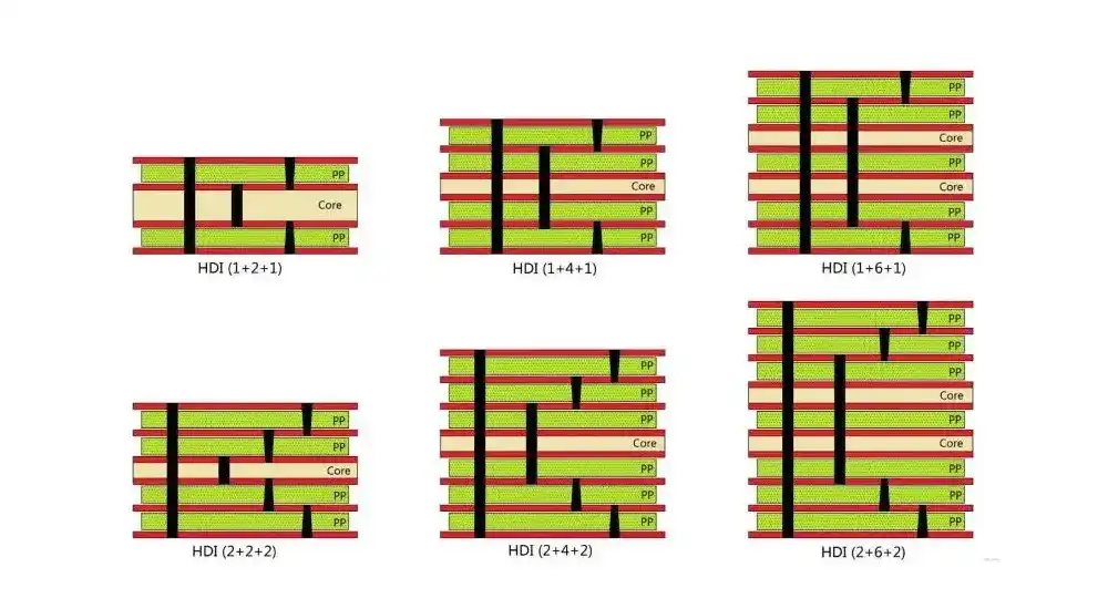
Layer configuration strategies in HDI designs follow standardized nomenclature systems that facilitate clear communication between design teams and manufacturing partners. The X-N-X format represents sequential lamination structures where the central N value indicates core layer count and the X values denote sequential lamination steps on each surface.
Configuration Selection Criteria
The selection of appropriate HDI stackup configurations requires careful analysis of component density requirements, routing complexity assessments, and thermal management considerations. Higher layer counts provide increased routing flexibility and enable more sophisticated power distribution networks, but introduce manufacturing complexity and cost implications that must be evaluated against performance benefits.
3. Microvia Technology Integration
Via Structure Types and Applications
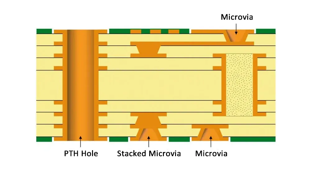
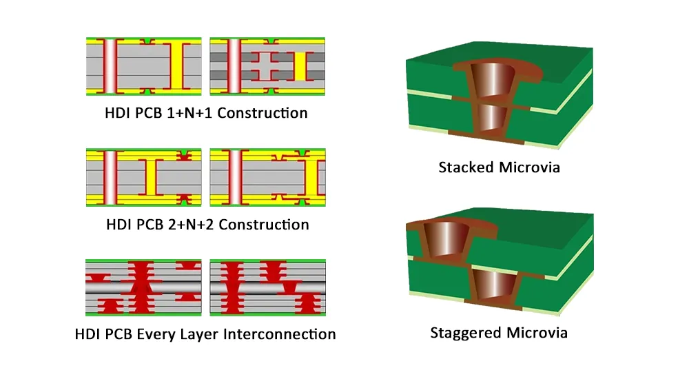
HDI PCB stackup designs employ various microvia configurations including stacked, staggered, and skip via arrangements. Each configuration offers distinct advantages for specific routing requirements and manufacturing constraints. Stacked vias provide direct layer-to-layer connections through multiple sequential laminations, while staggered configurations offer routing flexibility with reduced manufacturing complexity.
Aspect Ratio Considerations
The aspect ratio limitations of laser-drilled microvias significantly influence HDI stackup design decisions. Current manufacturing capabilities typically maintain aspect ratios below 1:1, with industry standards targeting 0.75:1 ratios to ensure reliable copper plating and electrical performance.
HDI PCB Stackup Types and Classification Systems
1. IPC Standard Classification Framework
Type I HDI Stackup Configuration
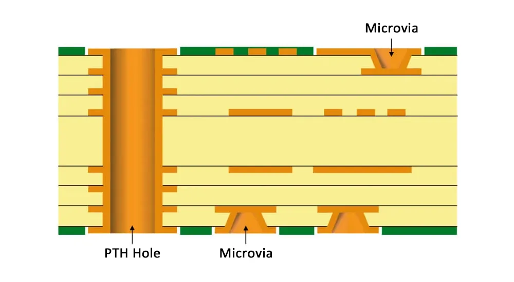
The IPC-2315 standard establishes six distinct HDI stackup types, with Types I, II, and III representing the most commonly implemented configurations in commercial applications. Type I HDI stackup features the simplest structure, incorporating a laminated core with at least one microvia layer on either one or both sides of the board. This configuration utilizes plated through-hole vias and blind vias while excluding buried vias from the design.
The primary limitation of Type I stackup stems from the aspect ratio constraints of plated through-hole vias, which must maintain ratios below 10:1 to ensure acceptable reliability levels. This restriction significantly impacts the scalability of Type I designs for large, dense boards incorporating multiple high-pin-count ball grid arrays. The single microvia layer limitation prevents Type I from achieving the routing density advantages that define advanced HDI implementations.
Type II HDI Stackup Characteristics
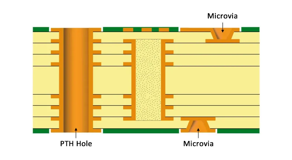
Type II HDI stackup represents an evolutionary advancement over Type I, incorporating microvias, blind vias, and buried vias within a laminated core structure. This configuration maintains at least one microvia layer on one or both sides while enabling staggered microvia arrangements relative to buried vias. The inclusion of buried vias provides significant advantages in overall board thickness reduction and enables smaller via diameters compared to Type I implementations.
While Type II stackup offers substantial improvements for large dense boards incorporating multiple fine-pitch components, it retains the same fundamental limitations as Type I regarding the number of laminated core layers. The enhanced routing capabilities provided by buried vias partially offset these limitations, making Type II suitable for moderate complexity applications requiring improved space utilization.
Type III HDI Stackup for Complex Applications
Type III HDI stackup provides the optimal configuration for large, dense multilayer PCBs incorporating multiple high-pin-count BGAs with pitches of 0.8mm or lower. This advanced configuration supports two or more microvia layers on at least one side of the board, enabling sophisticated via arrangements including stacked and staggered configurations that maximize routing flexibility.
The superior routing freedom provided by Type III stackup enables much thinner trace widths compared to either Type I or Type II configurations. This capability proves essential for applications requiring extreme miniaturization while maintaining signal integrity across high-speed interfaces. The ability to utilize surface layers for power or ground planes while dedicating inner layers to signal routing provides additional design optimization opportunities.
2. Sequential Lamination Classification System
M+N+M Structural Nomenclature
The sequential lamination classification system employs the M+N+M nomenclature where M represents the number of sequential lamination steps on each side of the core, and N indicates the core layer count. This standardized approach enables clear communication between design teams and manufacturing partners while facilitating accurate cost estimation and process planning.
The 2+N+2 configuration represents one of the most widely implemented HDI stackup types, incorporating two sequential lamination steps on each side of a conventional core structure. This approach provides an optimal balance between manufacturing complexity and design flexibility for moderate to high-density applications requiring enhanced routing capabilities.
Common Configuration Applications
The 1+N+1 stackup serves as the entry-level HDI configuration, providing cost-effective solutions for medium-density designs requiring fine-pitch component support. This configuration offers an ideal balance between cost and complexity while providing adequate support for fine-pitch components. The simplicity of single sequential lamination steps reduces manufacturing complexity and associated costs while delivering measurable improvements over traditional PCB approaches.
The 3+N+3 and higher configurations target high-complexity designs requiring advanced capabilities, though these approaches involve significantly higher costs due to increased manufacturing complexity. These advanced stackups enable sophisticated routing architectures essential for applications such as high-performance computing, advanced telecommunications infrastructure, and next-generation mobile devices requiring extreme component density.
3. Specialized HDI Stackup Variants
Every Layer Interconnect Technology
Every Layer Interconnect represents an advanced HDI variant enabling connections between any layer and any other layer through copper-filled microvias. This technology provides ultimate routing flexibility by eliminating traditional layer-to-layer connection constraints, enabling designers to optimize signal paths without regard to conventional stackup limitations.
The implementation of Every Layer Interconnect technology requires sophisticated manufacturing processes and advanced materials systems that significantly increase production complexity and costs. However, for applications demanding maximum routing density and signal optimization, this approach provides capabilities unattainable through conventional HDI stackup methods.
Passive Substrate and Standard Multilayer Variants
Passive Substrate HDI stackup typically incorporates a single HDI layer above or below core layers, enabling reduced PCB thickness compared to traditional multilayer approaches while concentrating high-density interconnects in specific regions. This approach proves particularly valuable for applications requiring localized high-density routing while maintaining cost-effectiveness for less critical circuit areas.
Standard Multilayer HDI construction follows conventional multilayer PCB methodologies while incorporating HDI layers on both sides of the core structure. This approach enables more complex routing and improved signal integrity through increased layer counts and interconnect densities. The balanced approach of Standard Multilayer configurations provides enhanced capabilities while maintaining manufacturing familiarity and process maturity.
Material Engineering and Manufacturing Process Optimization
Advanced Substrate Materials
High-Performance Dielectric Systems
Advanced material selection forms the technological foundation for HDI PCB stackup performance, requiring careful evaluation of dielectric properties, thermal characteristics, and processing compatibility. Modern HDI applications utilize specialized substrate materials including modified epoxy resins, polyimide films, and liquid crystal polymers that offer superior electrical properties compared to standard FR4 substrates.
Material Property Requirements
These advanced materials provide lower dielectric constants, reduced loss tangents, and enhanced thermal stability essential for high-frequency applications and dense component configurations. The selection process must account for frequency-dependent behavior, temperature stability, and compatibility with sequential lamination processes.
Sequential Lamination Manufacturing
Process Flow and Control Points
The manufacturing process for HDI PCB stackup designs involves sequential lamination techniques that enable precise control over layer thickness, material properties, and via formation. This process begins with core fabrication using conventional methods, followed by sequential addition of dielectric layers and copper foils.
Quality Assurance Systems
Quality control throughout the HDI manufacturing process requires advanced inspection and testing methodologies that can verify microvia formation quality, layer registration accuracy, and electrical connectivity integrity. These quality systems must address the unique challenges of HDI technology, including the verification of sub-surface features and the measurement of electrical properties at multiple intermediate stages.
Thermal Management Engineering
Heat Dissipation Strategies
Thermal management considerations become increasingly critical in HDI designs due to higher component densities and reduced surface areas available for heat dissipation. Strategic placement of thermal vias, optimized copper plane arrangements, and appropriate material selection help maintain operating temperatures within acceptable ranges.
Thermal Expansion Control
The coefficient of thermal expansion matching between different stackup materials prevents mechanical stress during temperature cycling, ensuring long-term reliability in demanding operating environments. This matching process requires careful selection of materials with compatible thermal properties throughout the stackup structure.
HDI Stackup Impedance Control and Signal Integrity Management
Controlled Impedance Design
Calculation Methodologies
HDI stackup impedance control represents one of the most critical aspects of high-density interconnect design, requiring precise calculation and verification of characteristic impedance values across all signal layers. The reduced layer spacing inherent in HDI designs significantly impacts impedance calculations, necessitating advanced electromagnetic field simulation tools for accurate predictions.
Manufacturing Sensitivity Analysis
The calculation of controlled impedance in HDI stackups involves complex interactions between trace geometry, dielectric properties, and adjacent conductor spacing. HDI configurations often feature spacing as low as 50 micrometers, making impedance control significantly more sensitive to manufacturing variations than traditional PCB designs.
Signal Integrity Optimization
Three-Dimensional Routing Advantages
Signal integrity optimization in HDI designs benefits from the three-dimensional routing capabilities enabled by microvia technology. The ability to transition between layers with minimal parasitic effects allows designers to optimize signal paths for improved performance characteristics.
High-Frequency Performance Characteristics
Reduced via stub lengths, achievable through controlled-depth drilling, significantly improve high-frequency performance compared to traditional through-hole vias. This advantage becomes particularly pronounced in applications operating beyond 1 GHz, including advanced memory interfaces and next-generation communication technologies.
Power Distribution Network Design
Distributed Decoupling Capabilities
Power distribution network design in HDI stackups requires specialized approaches that leverage the natural decoupling capabilities provided by thin dielectric layers. The close spacing between power and ground planes creates distributed capacitance that provides effective high-frequency noise filtering.
Resonance Management
This advantage must be balanced against increased susceptibility to plane resonances and their potential impact on power integrity across the frequency spectrum of interest. Careful modeling and design validation ensure optimal power delivery performance.
HDI Stackup vs Standard PCB Stackup: Comprehensive Analysis
Manufacturing Process Comparison
Sequential vs Traditional Lamination
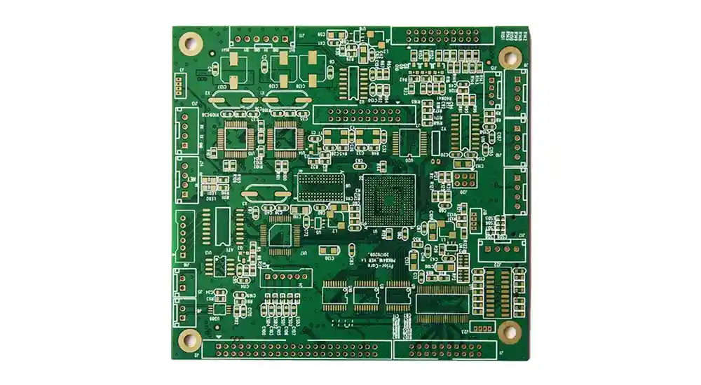
The distinction between HDI stackup vs standard PCB stackup extends far beyond simple manufacturing process differences, encompassing fundamental variations in electrical performance, design flexibility, and cost structures. Standard PCB fabrication follows subtractive manufacturing processes where all layers are laminated simultaneously, followed by mechanical drilling of through-holes.
Process Capability Advantages
HDI manufacturing employs sequential build-up methodologies that enable incremental layer addition with laser drilling performed at each stage. This process enables reduced drill aspect ratios, elimination of drill wandering common in thick boards, and the capability to create complex via structures.
Electrical Performance Analysis
Parasitic Element Reduction
Electrical performance differences between HDI and standard stackups manifest across multiple parameters that directly impact system performance. HDI designs typically exhibit lower parasitic inductance and capacitance due to shorter via lengths and optimized layer-to-layer spacing.
Space Utilization Efficiency
The space utilization efficiency of HDI stackups significantly exceeds that of standard designs, with the ability to route signals between any adjacent layers combined with the minimal footprint requirements of microvias enabling higher routing densities without corresponding increases in layer count.
Cost-Benefit Framework
Total System Cost Analysis
Cost-benefit analysis for HDI versus standard stackup selection requires comprehensive evaluation of total system costs rather than simple manufacturing cost comparisons. While HDI PCB stackup designs require higher initial investment, the total system cost often favors HDI implementations when considering all factors.
Value Proposition Elements
The elimination of expensive connectors, cable assemblies, and additional PCB layers in compact designs frequently provides cost advantages that offset manufacturing premiums. Enhanced reliability characteristics and improved electrical performance contribute additional value throughout the product lifecycle.
Advanced Applications and Design Optimization Strategies
Next-Generation Communication Systems
Millimeter-Wave Design Requirements
The implementation of HDI PCB stackup technology in next-generation communication systems requires sophisticated design approaches that accommodate millimeter-wave frequencies while maintaining acceptable signal loss characteristics. These applications demand extremely tight tolerance control and specialized low-loss materials.
Antenna Integration Technologies
Advanced antenna-in-package designs represent a growing application area where HDI technology enables the integration of radiating elements directly within the PCB stackup. This approach requires careful coordination between electromagnetic design requirements and manufacturing constraints.
Automotive and Aerospace Applications
Environmental Performance Requirements
Automotive and aerospace applications push HDI technology capabilities through demanding environmental requirements and ultra-high reliability standards. The automotive industry’s transition toward autonomous vehicles and electrification has created new demands for HDI PCB stackup designs capable of operating in harsh environments.
Weight and Space Optimization
Aerospace implementations extend these requirements through operation across extreme temperature ranges, radiation tolerance specifications, and weight optimization constraints where every gram impacts fuel efficiency and payload capacity.
Medical Device Integration
Biocompatibility and Reliability
Medical device applications increasingly rely on HDI PCB stackup technology to enable miniaturized implantable devices and sophisticated diagnostic equipment. These applications demand biocompatible materials, hermetic sealing capabilities, and long-term reliability in physiological environments.
Flexible HDI Implementations
The trend toward wearable medical devices has created opportunities for flexible HDI designs that combine the routing density advantages of traditional HDI with the mechanical flexibility required for body-worn applications through hybrid approaches.
Partnering with Haoyue Electronics for HDI Excellence
Engineering Expertise and Capabilities
The successful implementation of HDI PCB stackup technology requires more than advanced manufacturing capabilities; it demands deep engineering expertise, sophisticated process control, and comprehensive design optimization services. Haoyue Electronics has established itself as a leading provider of HDI PCB manufacturing and assembly services, combining state-of-the-art production facilities with extensive engineering experience.
Comprehensive Service Portfolio
Our engineering team collaborates closely with clients throughout the design optimization process, providing comprehensive design for manufacturability analysis, advanced signal integrity simulation, and cost optimization recommendations that ensure project success from concept through production. We maintain expertise across the complete spectrum of HDI technologies, from fundamental configurations to complex any-layer structures.
Commitment to Manufacturing Excellence
The Haoyue Electronics approach to HDI PCB stackup projects encompasses prototype development through high-volume production, ensuring that each project receives appropriate attention and expertise regardless of scale or complexity. Our comprehensive service portfolio includes design consultation, DFM analysis, advanced testing and validation, and complete turnkey manufacturing solutions.
Organizations seeking to leverage HDI PCB stackup technology for competitive advantage will find in Haoyue Electronics a partner committed to engineering excellence and manufacturing precision. Contact us today to discuss your specific requirements and discover how advanced HDI technology can transform your next project into a market-leading success.
From prototype to production — we help hardware teams cut costs, improve yields, and scale faster. Let’s make your next product a success!

