HDI PCB manufacturing represents a significant advancement over traditional PCB fabrication, incorporating microvias, sequential lamination, and laser drilling technologies to achieve interconnect densities that were previously impossible. This comprehensive guide examines the critical manufacturing processes, technical requirements, and quality considerations essential for successful HDI PCB production.
Understanding HDI PCB Architecture and Design Requirements
HDI Layer Structure Classifications
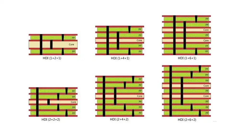
HDI printed circuit boards distinguish themselves through their sophisticated layer structures, typically classified using the industry-standard nomenclature of 1+N+1, 2+N+2, and 3+N+3 configurations. In this notation system, N represents the core layers while the numerical values indicate the number of sequential build-up layers added to each side.
Microvia Design Fundamentals
The fundamental design principle underlying HDI technology centers on microvia implementation. These laser-drilled interconnects, typically measuring between 50 to 150 micrometers in diameter, enable connections between adjacent layers without penetrating the entire board thickness. This selective connectivity allows designers to achieve higher routing density while reducing signal path lengths and improving electrical performance.
Critical Design Parameters
- Maintaining aspect ratios between 0.75:1 and 1:1 for microvias to ensure reliable plating
- Ensuring adequate copper thickness for reliable metallization processes
- Selecting materials compatible with multiple lamination cycles and thermal processing
- Careful consideration of via stacking versus staggering strategies based on density requirements
The design phase requires thorough evaluation of via stacking versus staggering strategies, with stacked configurations offering maximum density at the expense of increased processing complexity and cost considerations.
Advanced Materials Selection for HDI PCB Manufacturing
Material Performance Requirements
Successful HDI PCB manufacturing demands materials specifically engineered for high-temperature processing and dimensional stability. The material selection process requires careful evaluation of multiple performance criteria:
- Glass transition temperature (Tg) requirements typically exceeding 180°C to withstand multiple lamination cycles
- Coefficient of thermal expansion (CTE) remaining below 70 ppm/°C in the Z-axis direction to prevent delamination
- Dielectric constant stability across frequency ranges for high-speed applications
- Low loss tangent values (0.002 to 0.01) for signal integrity preservation
Industry-Proven Material Solutions
Industry-proven materials represent the foundation of reliable HDI manufacturing. Isola’s 370HR series provides exceptional thermal performance with a Tg of 180°C and superior CAF resistance for demanding applications. Panasonic’s Megtron family, particularly Megtron 6, 7, and 8, offers optimized properties for high-layer-count applications in networking and telecommunications equipment.
For applications requiring ultra-low loss characteristics, Rogers 4000 and 5000 series materials deliver controlled dielectric constants and excellent thermal stability across wide frequency ranges. These materials prove particularly valuable for RF and microwave applications where signal integrity requirements are paramount.
Laser Drilling Compatibility
The selection process must also consider laser drilling compatibility, as not all prepreg materials respond uniformly to laser ablation. Materials with homogeneous glass distribution and appropriate resin content facilitate consistent microvia formation and subsequent metallization processes. This compatibility directly impacts manufacturing yield and final product reliability.
Sequential Lamination: The Foundation of HDI Manufacturing
Process Overview and Methodology
Sequential lamination represents the most critical and complex aspect of HDI PCB manufacturing, involving multiple press cycles to build up the final board structure. This process begins with the fabrication of individual subsets, each comprising specific copper and dielectric layers that undergo independent processing before integration.
Detailed Lamination Process Steps
The typical sequential lamination process follows a carefully orchestrated sequence that ensures dimensional accuracy and layer registration:
- Initial positioning of copper foil and prepreg sheets on steel base plates with precise temperature control
- Careful alignment of pre-treated core layers using registration pins for accurate layer-to-layer positioning
- Addition of prepreg sheets and outer copper foil with contamination prevention measures
- Placement of aluminum press plates to ensure uniform pressure distribution and smooth copper finish
- Sequential processing of multiple subsets with intermediate quality verification steps
Critical Process Parameters
Critical process parameters require precise control throughout the lamination sequence. Press pressure maintains approximately 250 pounds per square inch for standard applications, with adjustments based on the cross-sectional area of the board stack-up. Temperature profiles must be precisely controlled to ensure complete resin cure while preventing copper oxidation or dimensional distortion.
The number of lamination cycles directly impacts both cost and reliability, with industry best practices recommending between two and three cycles for optimal results. Each additional cycle increases processing time and introduces potential registration errors, making careful stack-up planning essential for manufacturing efficiency.
Bonding and Curing Process
During the bonding process, heated press plates apply controlled pressure while temperature profiles reach curing temperatures for the epoxy resin systems. The cooling phase must be managed carefully to establish permanent layer bonding and minimize internal stress. Post-lamination cleaning removes oxide films, anti-foam residues, and contamination that could affect subsequent processing steps.
Laser Drilling Technology and Microvia Formation
Laser Technology Overview
Laser drilling technology enables the precise formation of microvias that define HDI capability. Two primary laser systems dominate HDI manufacturing: CO₂ lasers operating at 9.4 to 10.6 micrometer wavelengths for dielectric ablation, and UV lasers providing enhanced precision for smaller feature sizes.
CO₂ Laser Drilling Capabilities
CO₂ laser systems excel at dielectric material removal while leaving copper layers intact, making them ideal for blind microvia formation. These systems provide several distinct advantages:
- Creation of holes ranging from 50 to 70 micrometers in diameter with excellent repeatability
- Positional accuracy within ±3 mils for precise interconnect placement
- Non-contact processing that eliminates tool wear and contamination issues
- High throughput capability for production volume requirements
Advanced Laser Technologies
Advanced laser systems now achieve microvia diameters as small as 40 micrometers, with some equipment capable of simultaneous drilling from both sides of thin dielectric materials. This capability proves particularly valuable for substrate-like PCB applications where extreme miniaturization is required.
Process Optimization Requirements
Process optimization requires careful attention to multiple laser parameters:
- Pulse energy optimization to achieve clean hole profiles without thermal damage
- Repetition rate adjustment for consistent drilling speed and quality
- Beam focus control to maintain dimensional accuracy across panel areas
- Material-specific parameter development for different dielectric systems
Quality considerations include ensuring clean hole profiles without significant taper, minimizing heat-affected zones that could compromise subsequent plating processes, and maintaining consistent hole dimensions across large panel areas.
Microvia Metallization and Plating Excellence
Electroless Copper Deposition
Microvia metallization represents one of the most technically demanding aspects of HDI manufacturing, requiring specialized chemistry and process control to achieve reliable interconnections. The process begins with electroless copper deposition, which provides an initial conductive layer on the dielectric via walls.
The electroless copper process requires precise chemical composition and temperature control to ensure uniform deposition within the small microvia geometry. Bath chemistry must be optimized for throw power and throwing ability to reach the bottom of high-aspect-ratio features.
Electroplating Process Control
Electroplating follows electroless deposition to build copper thickness to specified requirements, typically 0.3 to 0.6 mils for wrap plating applications. The wrap plating technique extends copper deposition onto surface pads, creating robust mechanical and electrical connections between layers.
Process control parameters include several critical elements:
- Current density optimization to prevent throwing power issues and ensure uniform deposition
- Agitation control to ensure uniform chemistry distribution throughout the plating bath
- Temperature management to maintain consistent deposition rates and copper quality
- Chemistry monitoring to maintain optimal additive concentrations and metal content
Copper Filling for Stacked Microvias
For stacked microvia applications, copper filling becomes essential to provide a solid foundation for subsequent laser drilling operations. Specialized filling chemistry deposits copper from the via bottom upward, completely filling the microvia cavity. Post-fill planarization ensures a flat surface for subsequent layer addition.
Quality monitoring involves cross-sectional analysis to verify complete filling and adequate copper thickness distribution throughout the microvia structure.
Circuit Patterning and Fine Line Manufacturing
Laser Direct Imaging Technology
HDI PCB manufacturing demands exceptional precision in circuit patterning to achieve the fine line geometries necessary for high-density routing. Laser Direct Imaging (LDI) technology has become the standard for HDI applications, providing the resolution and registration accuracy required for features below 50 micrometers.
Advanced Patterning Processes
LDI systems eliminate the dimensional stability issues associated with photomasks while providing superior edge definition for fine lines and spaces. Modern LDI equipment achieves line width and spacing capabilities down to 25 micrometers with excellent uniformity across large panel areas.
The Semi-Additive Process (SAP) and modified Semi-Additive Process (mSAP) have gained prominence for ultra-fine line applications. These processes build copper circuitry through plating rather than etching, eliminating the undercutting and dimensional variations inherent in subtractive processes.
Manufacturing Environment Requirements
Clean room environments, typically Class 100 or better, are essential for HDI circuit patterning to prevent contamination that could cause yield issues. The fine feature sizes make these circuits particularly susceptible to particle contamination and chemistry variations that would be acceptable for standard PCB manufacturing.
Process optimization focuses on several key areas:
- Exposure energy management for optimal resist profile development
- Development uniformity across panel areas to ensure consistent line width control
- Resist profile control to achieve the dimensional accuracy required for fine pitch components
- Contamination prevention throughout the imaging and development sequence
Quality Control and Testing Methodologies
Automated Inspection Systems
HDI PCB manufacturing requires comprehensive quality control measures throughout the production process due to the critical nature of microvia connections and fine line circuitry. Automated Optical Inspection (AOI) systems provide 100% inspection of circuit features, with advanced algorithms capable of detecting defects below 10 micrometers.
X-Ray Inspection Capabilities
X-ray inspection proves essential for microvia quality assessment, particularly for filled and stacked configurations where conventional optical inspection cannot adequately evaluate internal structure. Modern X-ray systems provide sufficient resolution to detect voids, incomplete filling, and alignment issues within microvias.
Electrical Testing Requirements
Electrical testing requires specialized approaches for HDI PCBs due to the high interconnect density and small test access points:
- Flying probe testers with fine pitch capabilities enable comprehensive connectivity verification
- Specialized fixturing designed for specific HDI layouts when in-circuit testing is required
- Boundary scan testing for components with built-in test capabilities
- Functional testing protocols tailored to the specific application requirements
Process Validation Methods
Microsectioning and cross-sectional analysis provide critical process validation data, particularly for microvia plating quality and layer-to-layer registration accuracy. Statistical process control programs monitor key parameters including copper thickness distribution, via filling completeness, and dimensional accuracy trends.
Reliability testing protocols for HDI PCBs include thermal cycling to evaluate microvia integrity under temperature stress, mechanical testing to assess layer adhesion, and long-term aging studies to verify interconnect stability.
Cost Optimization Strategies for HDI PCB Manufacturing
Primary Cost Drivers
HDI PCB manufacturing costs reflect the complexity and precision required for successful production, but strategic optimization can significantly improve cost-effectiveness. The primary cost drivers include material selection, layer count, microvia complexity, and manufacturing yield considerations.
Lamination Cycle Optimization
Optimizing the number of lamination cycles provides the most significant cost reduction opportunity. Maintaining lamination cycles between two and three minimizes processing time while preserving signal integrity and reliability. Higher cycle counts exponentially increase processing complexity and associated costs.
Design Strategy Benefits
Design optimization strategies can significantly impact manufacturing costs:
- Minimizing stacked microvia usage in favor of staggered configurations where density requirements permit
- Optimizing panel utilization to maximize circuits per production panel
- Standardizing hole sizes and layer configurations to reduce setup complexity
- Balancing performance requirements with manufacturing constraints to optimize total cost
Material Selection Impact
Material selection impacts both initial costs and manufacturing yields. While advanced materials command premium pricing, their superior processing characteristics often result in higher yields and reduced rework costs. The total cost of ownership calculation should include yield improvements and reliability benefits when evaluating material options.
Manufacturing yield directly impacts unit costs, with even small improvements providing significant cost benefits. Investment in advanced process control equipment and comprehensive quality monitoring systems typically provides strong returns through yield improvement and reduced rework requirements.
Future Trends and Technology Advancement
Emerging Technologies
HDI PCB manufacturing continues to evolve rapidly, driven by demands for higher performance and greater miniaturization. Every Layer Interconnect (ELIC) technology represents the next frontier, enabling connections between any layers within the board structure through advanced microvia stacking techniques.
Advanced Manufacturing Capabilities
Emerging laser drilling technologies promise even smaller microvia diameters, with research systems demonstrating capabilities below 25 micrometers. Simultaneous dual-side drilling capabilities improve processing efficiency while enabling new design architectures previously impossible with single-side processing.
Intelligence and Automation
Artificial intelligence and machine learning applications are beginning to optimize HDI manufacturing processes through predictive analytics and real-time process adjustment. These systems analyze vast datasets to identify optimization opportunities and predict potential quality issues before they impact production.
Advanced materials development focuses on reducing dielectric loss while maintaining processability for high-frequency applications. New resin systems provide improved thermal performance and dimensional stability, enabling more aggressive HDI designs with enhanced reliability.
Conclusion: Excellence in HDI PCB Manufacturing
Manufacturing high-quality HDI PCBs demands expertise in advanced processes, materials, and quality control. Techniques like sequential lamination, laser drilling, and precise metallization enable the dense interconnections required for modern electronics.
As device miniaturization continues, HDI technology becomes essential for competitive products. Partnering with experienced manufacturers ensures consistent quality and successful outcomes.
At Haoyue Electronics, we invest in cutting-edge equipment and skilled engineers to deliver top-tier HDI PCB manufacturing and assembly. We collaborate closely with customers from design to final testing, optimizing for performance and manufacturability.
Whether you need prototypes or large-scale production, our commitment to quality and precision supports your project’s success. Contact us today to explore how we can help bring your HDI designs to life.
From prototype to production — we help hardware teams cut costs, improve yields, and scale faster. Let’s make your next product a success!

