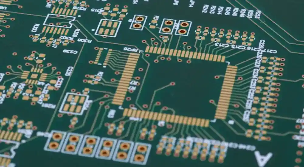
This comprehensive guide explores the technical progression from traditional 1.0mm pitch designs to cutting-edge 0.4mm implementations, providing engineers with practical insights for modern PCB development.
The transition from conventional through-hole via designs to sophisticated microvia architectures represents more than just a scaling challenge—it fundamentally reshapes how we approach signal integrity, thermal management, and manufacturing reliability in advanced electronic systems.
Understanding HDI Technology Evolution in BGA Design
The Foundation of Modern HDI Architecture
HDI PCB design guide principles have evolved significantly over the past decade, driven primarily by the semiconductor industry’s relentless push toward miniaturization. The fundamental shift from through-hole vias to microvia technology isn’t merely about space savings—it’s about maintaining signal integrity and reliability while achieving unprecedented component density.
Traditional PCB design methodologies, which relied heavily on through-hole vias with 6:1 to 8:1 aspect ratios, face inherent limitations when addressing fine-pitch BGA components. The physics of copper plating in deep, narrow holes creates reliability concerns, particularly under thermal cycling conditions where differential expansion coefficients between copper and FR4 substrate materials can lead to barrel cracking.
Microvia Technology: The Game Changer
Microvia technology fundamentally addresses these limitations through laser-drilled structures typically limited to 100μm depth. This shallow architecture eliminates the thermal stress issues associated with deep through-hole vias while enabling the precise placement required for fine-pitch routing. The 1:0.8 aspect ratio commonly used in modern microvia designs provides optimal reliability while maximizing routing density.
| Technology Comparison | Through-Hole Vias | Microvias |
|---|---|---|
| Maximum Depth | 1.6mm+ | 100μm typical |
| Aspect Ratio | 6:1 to 8:1 | 1:0.8 |
| Minimum Diameter | 0.25mm | 0.1mm |
| Thermal Stress | High (barrel cracking risk) | Low |
| Signal Integrity | Moderate (higher parasitic) | Excellent |
| Manufacturing Cost | Lower | Higher |
| Reliability (Class 3) | Good (with proper design) | Excellent |
| Fine-Pitch Compatibility | Limited | Excellent |
1.0mm Pitch BGA: Foundation Design Principles
Establishing Baseline Design Parameters
The 1.0mm pitch BGA represents the transition point where designers can choose between traditional through-hole via approaches and modern HDI techniques. For lower complexity designs with PCB thickness up to 1.6mm and layer counts below 8, through-hole vias remain viable when properly implemented.
| Design Parameter | Specification | Standard Reference |
|---|---|---|
| Via Pad Diameter | 0.55-0.60mm | IPC-2221A compliant |
| Minimum Drill Diameter | 0.25mm | IPC-2221A |
| Solder Mask Clearance | 50μm minimum | Industry standard |
| Track Width/Spacing (Outer) | 100μm | Standard capability |
| Track Width/Spacing (Inner) | 100μm | Standard capability |
| Maximum PCB Thickness | 1.6mm | Through-hole via compatibility |
| Recommended Layer Count | ≤8 layers | Complexity limitation |
Design Decision Matrix
| Selection Criteria | Through-Hole Vias | Microvias | Recommendation |
|---|---|---|---|
| PCB Thickness | <1.6mm | Any | Through-hole for thin PCBs |
| Layer Count | ≤8 layers | Any | Through-hole for simple designs |
| Component Density | Low-Medium | High | Microvias for dense layouts |
| Signal Frequency | <1GHz | >1GHz | Microvias for high-speed |
| Cost Sensitivity | High | Medium-Low | Through-hole for cost optimization |
| Future Scalability | Limited | Excellent | Microvias for design evolution |
| Manufacturing Volume | High | Any | Consider economics at scale |

0.8mm to 0.65mm Pitch: Transitioning to Microvia Solutions
The Critical Transition Zone
The 0.8mm to 0.65mm pitch range represents a critical transition where microvia technology becomes increasingly necessary for reliable, manufacturable designs. This section explores the three primary architectural approaches and their optimization strategies.
Variant Analysis: Dogbone vs. Via-in-Pad
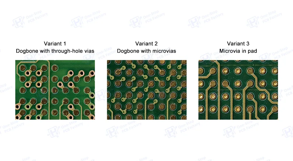
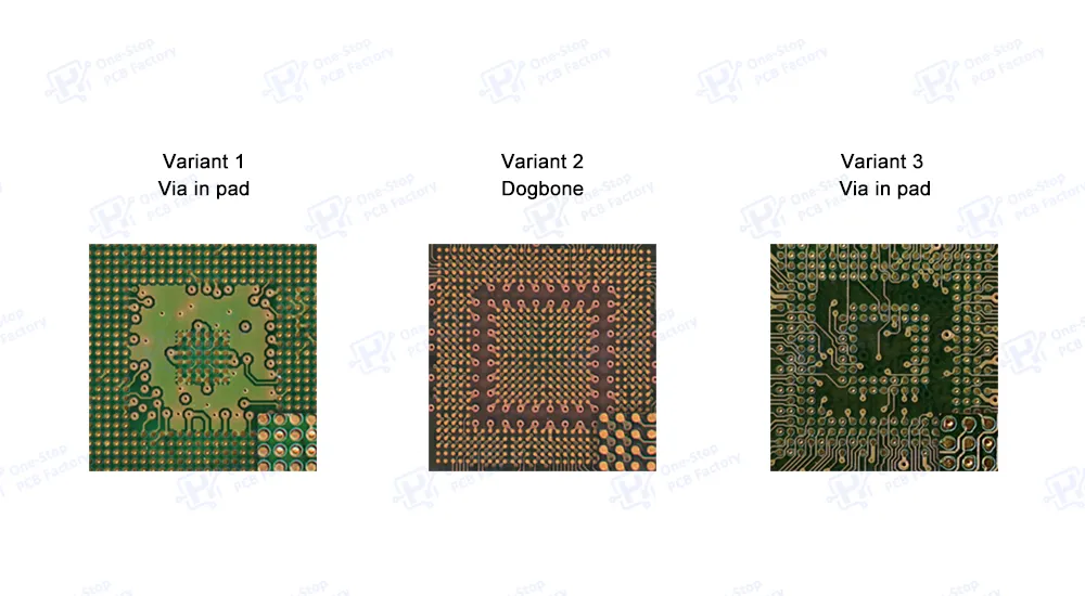
1. Dogbone Configuration with Through-Hole Vias
For 0.8mm pitch applications, dogbone routing with reduced via pad sizes (0.50mm) remains feasible for limited complexity designs. However, this approach requires careful tolerance management and is generally recommended only for PCB thickness below 1.8mm with maximum 12-layer stackups.
2. Dogbone Configuration with Microvias
This configuration offers the advantage of planar solder pad surfaces, minimizing voiding risks during reflow soldering. The approach facilitates improved solder joint formation but limits outer layer routing flexibility between BGA pads.
3. Via-in-Pad Microvia Implementation
The most widely adopted solution for 0.8mm pitch designs, via-in-pad microvias maximize routing efficiency while maintaining acceptable solder joint quality. Modern reflow profiles can effectively manage the minor dimpling effects, though microvia filling processes may be employed for critical applications.

Advanced Design Parameters for 0.65mm Pitch
At 0.65mm pitch, microvia implementation becomes mandatory for reliable designs. The reduced available real estate demands precise parameter optimization:
| Design Parameter | 0.8mm Pitch | 0.65mm Pitch | Critical Notes |
|---|---|---|---|
| BGA Solder Pad | 400μm | 350μm | NSMD preferred |
| Solder Mask Clearance | 50μm | 50-65μm | Tighter tolerance required |
| Track Width (Outer) | 100μm | 100-125μm | Standard capability maintained |
| Track Width (Inner) | 100μm | 90-100μm | May require fine-line |
| Microvia Pad (Outer) | 300-350μm | 300-350μm | Consistent sizing |
| Microvia Pad (Inner) | 300-350μm | 300-350μm | Consistent sizing |
| Manufacturing Complexity | Medium | Medium-High | Registration critical |
Detailed Variant Comparison for 0.8mm Pitch
| Parameter | Variant 1: Dogbone + PTH | Variant 2: Dogbone + Microvia | Variant 3: Via-in-Pad |
|---|---|---|---|
| BGA Solder Pad | 400μm max | Not applicable | 500μm max |
| Solder Mask Clearance | 50μm | ≥50μm | 50μm |
| Via Pad Size (BGA Area) | 500μm | Not applicable | Not applicable |
| Microvia Pad (Outer) | Not applicable | 300/350μm | 300/350μm |
| Microvia Pad (Inner) | Not applicable | 300/350μm | 300/350μm |
| Track Width (Outer) | ≥100μm | ≥100μm | ≥100μm |
| Track Width (Inner) | ≥100μm | ≥100μm | ≥100μm |
| Surface Planarity | Standard | Excellent | Good (minor dimpling) |
| Routing Flexibility | Limited | Limited | Excellent |
| Solder Joint Quality | Good | Excellent | Good |
| Manufacturing Cost | Lowest | Medium | Medium |
0.5mm Pitch BGA: Advanced Fine-Line Techniques
Engineering at the Limits
The 0.5mm pitch threshold demands sophisticated HDI design techniques and represents the boundary where conventional manufacturing approaches reach their practical limits. Success at this pitch requires careful consideration of three distinct architectural variants, each optimized for specific application requirements.

Comprehensive Variant Analysis for 0.5mm Pitch
| Parameter | Variant 1: Conservative | Variant 2: Planar Surface | Variant 3: Maximum Density |
|---|---|---|---|
| BGA Solder Pad | 300-330μm | 240μm | 275μm |
| Solder Mask Clearance | 50μm | 40μm | 35μm |
| Microvia Pad (Outer) | ≥300μm | 275μm | 275μm |
| Microvia Pad (Inner) | 275μm | 275μm | 275μm |
| Track Width (Outer) | ≥100μm | 80/90μm | 75μm |
| Track Width (Inner) | 75μm | 75μm | 75μm |
| Copper Thickness Limit | 25μm final | 25μm final | 18μm final |
| Manufacturing Complexity | Medium | High | Highest |
| Solder Joint Quality | Good | Excellent | Good |
| Routing Efficiency | Medium | Low | Highest |
| Cost Impact | Medium | High | Highest |
Fine-Line Manufacturing Requirements
| Process Parameter | Standard PCB | 75μm Fine-Line | Impact |
|---|---|---|---|
| Lithography Resolution | 100μm | 75μm | Enhanced equipment required |
| Registration Tolerance | ±50μm | ±25μm | Tighter process control |
| Etching Chemistry | Standard | Modified | Aspect ratio optimization |
| Copper Thickness | 35μm+ | 18-25μm | Limited current capacity |
| Inspection Protocol | Standard AOI | Enhanced AOI + SEM | Increased inspection time |
| Yield Impact | Baseline | 10-15% reduction | Economic consideration |
| Equipment Investment | Standard | High-end lithography | Capital cost increase |
0.4mm Pitch and Beyond: Cutting-Edge HDI Strategies
Pushing Technology Boundaries
The 0.4mm pitch represents the current frontier of production HDI technology, requiring advanced techniques such as stacked microvias and filled via processes. These implementations demand sophisticated manufacturing capabilities and represent significant engineering investments.
Technical Specifications for 0.4mm Pitch
| Design Parameter | Standard Specification | Advanced Option | Notes |
|---|---|---|---|
| BGA Solder Pad | 275μm | 250μm | NSMD mandatory |
| Solder Mask Clearance | 35μm | 30μm | Precision lithography required |
| Microvia Pad (Inner) | 300μm | 275μm | Filled vias recommended |
| Track Width (All Layers) | ≥100μm | 75μm | Standard vs. fine-line |
| Via Filling | Optional | Mandatory | Inner layer microvias |
| Layer Count | 8-12 | 12-20 | Complexity dependent |
| Dielectric Thickness | 85-110μm | 75-100μm | Controlled prepreg |
Stacked Microvia Architecture Comparison
| Architecture Type | Layer Transition | Complexity | Cost Impact | Reliability | Applications |
|---|---|---|---|---|---|
| Single Microvia | L1-L2, L2-L3 | Low | Baseline | Good | Simple designs |
| Staggered Microvias | Offset positioning | Medium | +25% | Better | Medium complexity |
| Stacked Microvias | Direct alignment | High | +50% | Excellent | High density |
| Skip Via (1+N+1) | L1-L3, L3-L5 | Medium | +30% | Good | Optimized routing |
Manufacturing Process Requirements
| Process Step | Standard HDI | 0.4mm Pitch | Equipment Upgrade |
|---|---|---|---|
| Laser Drilling | CO2 laser | UV laser preferred | Higher precision required |
| Registration Accuracy | ±25μm | ±15μm | Enhanced alignment systems |
| Lamination Tolerance | ±10μm | ±5μm | Precision press required |
| Inspection Resolution | 10μm | 5μm | Advanced AOI/X-ray |
| Via Filling Process | Optional | Mandatory | Additional process step |
| Layer Count Capability | 12 layers | 20+ layers | Sequential build-up |
Design Optimization and Manufacturing Considerations
Holistic Design Approach
Successful HDI PCB design for fine-pitch BGA applications requires integration of electrical, mechanical, and manufacturing considerations throughout the design process. This section explores optimization strategies that ensure both performance and manufacturability.
Signal Integrity Optimization Parameters
| Parameter | Standard PCB | Fine-Pitch HDI | Optimization Strategy |
|---|---|---|---|
| Via Inductance | 1-2 nH | 0.3-0.8 nH | Microvia implementation |
| Via Capacitance | 0.5-1 pF | 0.2-0.5 pF | Reduced via pad size |
| Impedance Control | ±10% | ±5% | Controlled dielectric thickness |
| Crosstalk | -30 dB | -40 dB | Tighter spacing control |
| Return Loss | -15 dB | -20 dB | Via stub elimination |
| Insertion Loss | 0.5 dB/inch | 0.3 dB/inch | Shorter via barrels |
Cost Optimization Matrix
| BGA Pitch | Architecture Choice | Relative Cost | Complexity Level | Recommended Volume |
|---|---|---|---|---|
| 1.0mm | Through-hole vias | 1.0x (baseline) | Low | >10,000 units |
| 1.0mm | Microvias | 1.2x | Medium | Any volume |
| 0.8mm | Dogbone + microvias | 1.4x | Medium | >5,000 units |
| 0.8mm | Via-in-pad | 1.5x | Medium-High | >2,000 units |
| 0.65mm | Microvias | 1.6x | High | >1,000 units |
| 0.5mm | Conservative approach | 1.8x | High | >500 units |
| 0.5mm | Fine-line implementation | 2.2x | Very High | >100 units |
| 0.4mm | Stacked microvias | 2.8x | Extreme | Prototype/Low volume |
Manufacturing Quality Assurance Protocol
| Inspection Level | BGA Pitch Range | Test Methods | Acceptance Criteria | Frequency |
|---|---|---|---|---|
| Level 1: Standard | 1.0mm - 0.8mm | AOI + Flying Probe | IPC-A-610 Class 2 | 100% AOI, 10% electrical |
| Level 2: Enhanced | 0.65mm - 0.5mm | AOI + ICT + X-ray | IPC-A-610 Class 3 | 100% AOI/X-ray, 25% electrical |
| Level 3: Premium | 0.4mm and below | AOI + ICT + X-ray + SEM | Custom specifications | 100% all methods |
Thermal Management Strategy Guide
| Component Density | Power Dissipation | Thermal Via Strategy | Layer Stackup Consideration |
|---|---|---|---|
| Low (<5 W) | Standard | Optional thermal vias | Standard stackup |
| Medium (5-15 W) | Enhanced | 0.2mm thermal vias, 0.5mm spacing | Copper pour optimization |
| High (15-30 W) | Advanced | 0.15mm thermal vias, 0.3mm spacing | Dedicated thermal layers |
| Extreme (>30 W) | Specialized | Filled thermal vias + heat spreader | Metal core integration |
Future Technology Readiness Assessment
| Technology | Current Status | 0.4mm Compatibility | 0.3mm Potential | Timeline |
|---|---|---|---|---|
| Embedded Components | Limited production | Good | Excellent | 2-3 years |
| Glass Substrates | R&D phase | Excellent | Excellent | 3-5 years |
| Additive Manufacturing | Prototype | Good | Good | 5-7 years |
| 3D Printed Electronics | Research | Limited | Good | 7-10 years |
| Quantum Interconnects | Early research | Not applicable | Limited | 10+ years |
Conclusion: Strategic Implementation for Success
The progression from 1.0mm to 0.4mm BGA pitch represents more than a simple scaling exercise—it embodies a fundamental transformation in PCB design methodology. Success in this evolution requires understanding not just the technical specifications, but the interdependencies between design decisions, manufacturing capabilities, and application requirements.
Modern HDI PCB design guide principles emphasize the importance of early collaboration between design teams and manufacturing partners. The complexity of fine-pitch implementations demands this partnership approach to ensure both technical success and economic viability.
As we continue to push the boundaries of electronic miniaturization, the principles established in this pitch evolution will form the foundation for even more advanced implementations. The key to success lies in understanding these fundamentals while remaining adaptable to emerging technologies and changing application requirements.
Haoyue Electronics specializes in advanced HDI PCB manufacturing and assembly services, supporting the full spectrum of BGA pitch requirements from conventional 1.0mm implementations to cutting-edge 0.4mm designs. Our comprehensive capabilities include fine-line processing, microvia technology, and sophisticated assembly services designed to meet the most demanding electronic applications.
Contact us for your next HDI PCB project!
From prototype to production — we help hardware teams cut costs, improve yields, and scale faster. Let’s make your next product a success!

