Why Choose HDI PCB Over Ordinary PCB
Key Differences in Technology
HDI PCBs utilize microvias instead of traditional through-hole vias, enabling significantly higher routing density. While ordinary PCBs use vias with diameters of 200 micrometers or larger, HDI technology employs microvias under 150 micrometers, allowing finer component placement and more efficient board space utilization.
Performance Advantages
HDI designs achieve the same functionality as conventional boards using fewer layers, reducing material costs and improving electrical performance through shorter signal paths. A typical 8-layer conventional design can often be replaced by a 6-layer HDI board with superior performance characteristics.
Applications and Benefits
HDI technology provides superior electrical performance through reduced parasitic effects and shorter interconnect lengths. This results in lower inductance and capacitance, improving signal integrity and reducing electromagnetic interference for high-speed digital applications.
Microvia Technology Fundamentals
Basic Microvia Characteristics
Microvias are precision-drilled holes created using laser drilling processes, achieving diameters between 50 and 150 micrometers. Unlike mechanical drilling, laser drilling enables very small holes without tool wear limitations and provides exceptional accuracy and consistency.
Aspect Ratio Requirements
The aspect ratio of microvias must be maintained below 1:1 for optimal manufacturing reliability. This means a microvia drilled through a 75-micrometer dielectric layer requires a diameter of at least 75 micrometers to ensure reliable copper plating and electrical continuity.
Microvia Filling Considerations
Copper-filled microvias provide superior electrical conductivity and mechanical strength, particularly important for stacked configurations. However, the filling process adds manufacturing steps and cost, requiring careful consideration of performance requirements versus economic factors.
Strategic Positioning
Proper microvia placement enables efficient component fanout, especially for fine-pitch ball grid array packages where conventional via technology proves inadequate. Strategic positioning also facilitates power and ground distribution in high-density layouts.

Stackup Structure Types and Selection
1-N-1 Configuration
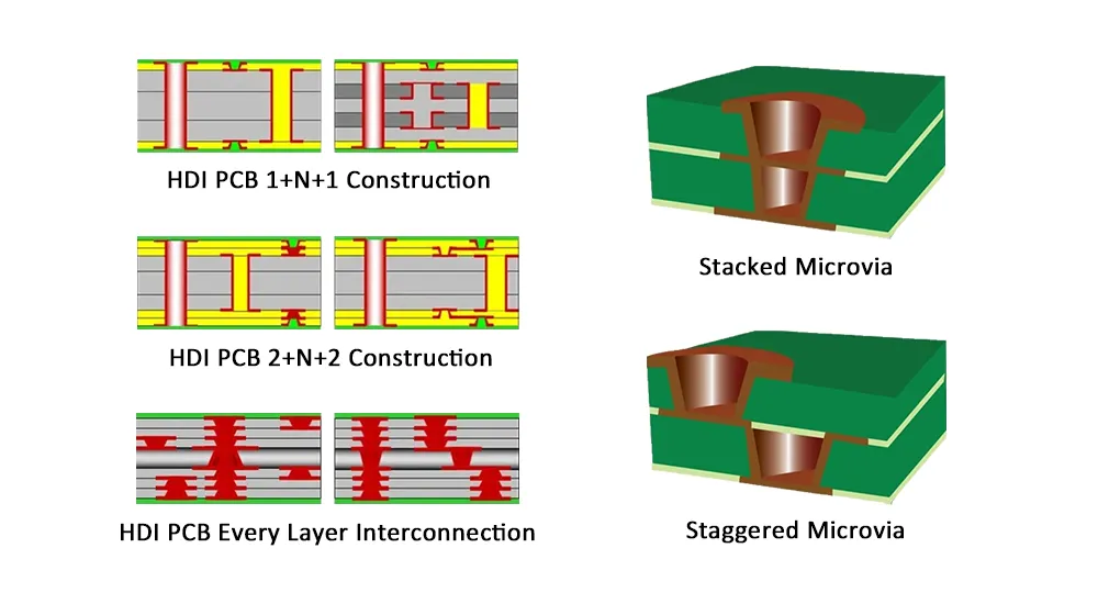
The most common HDI structure features one microvia layer on each side of a conventional multilayer core. This approach provides moderate routing density improvement while maintaining compatibility with established manufacturing processes and reasonable cost structures.
Advanced Configurations (2-N-2 and Higher)
Higher-order stackups enable greater routing density through multiple sequential lamination cycles. Each additional build-up layer increases manufacturing complexity and cost while providing proportional improvements in routing capability.
Every Layer Interconnect (ELIC)
ELIC structures represent the most advanced HDI configuration, enabling microvia connections between any layers within the stackup. This approach provides maximum routing flexibility for extremely complex designs but requires sophisticated manufacturing processes and premium pricing.
Selection Criteria
Stackup complexity selection depends on component density requirements, routing challenges, and project budget constraints. Understanding the cost-performance trade-offs helps designers make appropriate decisions based on specific project requirements.
Material Selection Fundamentals
Standard vs. Advanced Materials
Standard FR-4 materials remain suitable for many HDI applications operating at moderate frequencies and temperatures. Advanced applications often require specialized resin systems with improved electrical properties, such as modified polyimide or low-loss thermosetting materials.
Thermal Considerations
HDI designs require materials with enhanced thermal conductivity due to higher component density and reduced board thickness. Low coefficient of thermal expansion reduces stress on microvia structures during thermal cycling.
Electrical Properties
Dielectric constant and loss tangent specifications become critical for high-speed HDI applications. Lower dielectric constants enable controlled impedance design with wider trace geometries, while reduced loss tangents minimize signal attenuation.
Selection Guidelines
Material selection must balance thermal performance requirements with electrical properties and manufacturing compatibility. Understanding these trade-offs enables optimal performance while maintaining manufacturing feasibility.
Choosing the right materials is key to HDI PCB performance and reliability. For a detailed technical guide, see:
Design Rules and Layout Guidelines
Geometric Constraints
HDI design rules specify minimum trace widths of 75 micrometers or less, with corresponding spacing requirements that accommodate manufacturing tolerances. These reduced geometries enable higher routing density but require precise manufacturing processes.
Pad Size Optimization
Microvia capture pads typically measure 200 to 250 micrometers in diameter, significantly smaller than conventional via pads. Component pad sizes must accommodate both assembly requirements and routing constraints.
BGA Fanout Strategies
Microvia technology enables dog-bone fanout patterns that route signals directly from BGA pads to inner layers without consuming excessive routing area. Strategic via placement ensures efficient signal distribution while maintaining signal integrity.
Microvia Arrangement Patterns
Staggered microvia configurations distribute drilling loads across multiple layers, improving manufacturing yield. Stacked arrangements provide more direct routing paths and conserve board area but require copper filling for reliability.
Manufacturing Process Overview
Sequential Build-up Process
HDI manufacturing employs sequential lamination cycles that add dielectric layers and microvia structures to a traditional multilayer core. Each cycle includes dielectric application, laser drilling, desmear treatment, and copper plating processes.
Laser Drilling Technology
Carbon dioxide and ultraviolet laser systems provide precision microvia formation with different advantages for various materials. Process parameters must be optimized for each material combination to achieve consistent results.
Quality Control Requirements
Manufacturing quality control requires specialized inspection and testing procedures. Microvia formation assessment employs optical and X-ray inspection systems, while electrical testing validates interconnect continuity and insulation resistance.
Registration Accuracy
Layer-to-layer registration becomes critical as stackup complexity increases, requiring advanced tooling and measurement systems to maintain manufacturing tolerances throughout the build-up process.
Signal Integrity and Thermal Management Basics
Signal Integrity Considerations
Reduced trace geometries and increased routing density create potential electromagnetic interference and crosstalk issues. Proper routing techniques and stackup design help maintain signal quality while maximizing routing efficiency.
Controlled Impedance Design
HDI designs require precise specification of trace width, dielectric thickness, and copper weight parameters. The reduced geometries can make impedance control more challenging, requiring tighter manufacturing tolerances.
Thermal Management Strategies
Increased power density and reduced heat dissipation area require careful thermal management. Component placement strategies must consider thermal coupling effects and heat flow paths to prevent localized overheating.
Power Delivery Networks
Power distribution design must accommodate increased current density requirements within HDI geometric constraints. Plane layer optimization, via stitching, and embedded capacitor technologies help maintain power integrity.
Summary
Technology Benefits
HDI PCB technology offers significant advantages through improved routing density, enhanced electrical performance, and reduced form factors. Successful implementation requires understanding microvia technology, appropriate stackup selection, and careful attention to design rules.
Implementation Considerations
The transition to HDI design involves learning new methodologies and manufacturing considerations that impact both technical performance and project economics. Material selection, thermal management, and signal integrity requirements become more critical.
Design for Manufacturing
Collaboration between design and manufacturing teams proves essential for successful HDI implementation. Early consideration of manufacturing constraints helps avoid costly redesign cycles while ensuring optimal performance and reliability.
Future Applications
As electronic devices continue demanding improved performance within smaller form factors, HDI technology remains essential for competitive product development across consumer electronics, high-performance computing, and telecommunications applications.
From prototype to production — we help hardware teams cut costs, improve yields, and scale faster. Let’s make your next product a success!

