Understanding FR4 PCB Warping and Industry Standards
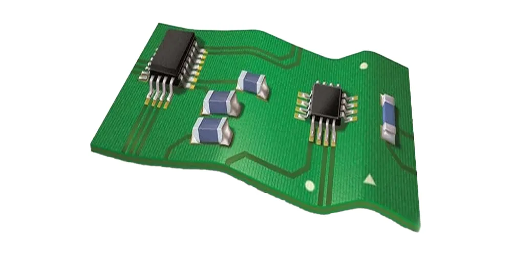
FR4 PCB warping refers to the deviation of a printed circuit board from its intended flat configuration, manifesting as bowing, twisting, or bending that compromises assembly processes and final product integrity. This PCB flatness issue affects surface mount technology placement accuracy, solder joint quality, and overall circuit reliability.
IPC-6012 PCB Warpage Standards
Industry standards define acceptable limits for PCB board warping. According to IPC-6012 classification, maximum allowable warpage differs based on component requirements:
- Surface Mount Applications: Maximum 0.75% warpage tolerance
- Through-Hole Components: Maximum 1.5% warpage tolerance
- High-Precision Assembly: Often requires 0.5% or stricter tolerances
The warpage calculation follows IPC-TM-650.2.4.22B methodology, measuring the maximum deviation height against the PCB diagonal length. Many advanced electronic assembly facilities now demand even tighter specifications, with some requiring 0.3% maximum warpage for critical applications.
Impact on Assembly Processes
FR4 PCB deformation creates multiple manufacturing challenges that extend beyond simple aesthetics. Component placement accuracy suffers when boards cannot maintain proper flatness during pick-and-place operations. Solder joint integrity becomes compromised when uneven board surfaces prevent proper component seating. Wave soldering processes experience reduced effectiveness when warped boards prevent consistent pad contact with molten solder.
Root Causes of FR4 PCB Warping
Understanding the fundamental mechanisms behind FR4 PCB warping enables effective prevention strategies. Multiple factors contribute to board deformation, often working in combination to create warpage issues.
Thermal Expansion Coefficient Mismatch
FR4 material exhibits anisotropic thermal expansion characteristics, expanding differently along X, Y, and Z axes when exposed to temperature variations. The glass transition temperature (Tg) represents a critical threshold where FR4 transitions from rigid to flexible behavior. Standard FR4 materials typically exhibit Tg values between 130-140°C, while high-Tg variants reach 170-180°C.
When FR4 PCBs experience temperatures approaching or exceeding their Tg values during reflow soldering, the material becomes susceptible to permanent deformation. The coefficient of thermal expansion (CTE) increases dramatically above the Tg point, making boards vulnerable to stress-induced warping.
Copper Distribution Asymmetry
Uneven copper surface area distribution creates thermal and mechanical stress imbalances that promote FR4 PCB bending. Large copper planes on one layer without corresponding copper on opposite layers generate differential thermal expansion during temperature cycling. This asymmetry becomes particularly problematic when power planes or ground planes occupy significant portions of specific layers while leaving other layers relatively sparse.
The copper thickness variation across different board areas compounds this issue. Thick copper regions (2oz or greater) exhibit different thermal behavior compared to standard 1oz copper areas, creating localized stress concentrations that contribute to board warping.
Manufacturing Process Stresses
The PCB fabrication process introduces inherent stresses that remain locked within the FR4 laminate structure. Press lamination cycles, drilling operations, and chemical processing create residual stresses that may not manifest immediately but contribute to delayed warpage under subsequent thermal exposure.
Prepreg material selection and layup symmetry significantly influence final board stability. Asymmetric stackups, particularly those with unequal prepreg distribution or varying core thicknesses, create mechanical imbalances that predispose boards to warping under thermal stress.

Why FR4 PCBs Warp During Reflow Soldering
Reflow soldering presents the most critical thermal challenge for FR4 PCB flatness maintenance. The combination of elevated temperatures, extended exposure times, and mechanical constraints creates ideal conditions for board deformation.
Temperature Profile Impact
Modern lead-free reflow profiles require peak temperatures between 250-260°C, significantly exceeding the Tg of standard FR4 materials. During the ramp-up phase, differential thermal expansion between copper and FR4 substrate creates internal stresses. The soaking phase allows these stresses to redistribute, while the peak temperature phase approaches or exceeds material limits.
The cooling phase proves equally critical for maintaining board flatness. Rapid cooling can lock in thermal stresses, while controlled cooling allows gradual stress relief. Board support during cooling becomes essential for preventing permanent deformation as the FR4 material transitions back below its Tg point.
Mechanical Support Considerations
Reflow oven conveyor systems typically support boards at their edges, creating a cantilever effect for large or heavy boards. This support configuration concentrates mechanical stress at support points while allowing central areas to sag under their own weight when heated above the Tg threshold.
Component weight distribution affects warping tendencies during reflow processing. Large components, particularly BGA packages or heavy connectors, create localized stress concentrations that can initiate board bending. Asymmetric component placement exacerbates these effects by creating unbalanced loading conditions.
Panel Design Influences
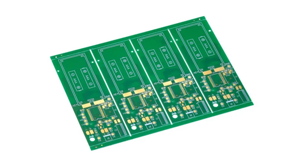
V-cut scoring and tab routing significantly compromise board structural integrity. V-cuts create stress concentration points that weaken the overall panel structure, making individual boards more susceptible to warping during thermal processing. The depth and angle of V-cuts directly correlate with warpage susceptibility.
Panel size optimization requires balancing manufacturing efficiency with thermal stability. Larger panels improve throughput but increase warpage risk due to increased unsupported areas and greater thermal mass variations across the panel surface.
Design Solutions to Prevent FR4 PCB Warping
Effective warpage prevention begins during the design phase, where careful attention to material selection, stackup design, and component placement can minimize warping tendencies.
Material Selection and Stackup Optimization
High-Tg FR4 materials provide superior thermal stability for applications experiencing elevated operating temperatures or aggressive reflow profiles. Materials with Tg values exceeding 170°C maintain dimensional stability throughout standard reflow processes, reducing warpage risk significantly.
Symmetric stackup design proves essential for balanced thermal expansion behavior. Mirror-image layer arrangements ensure equal copper distribution above and below the board centerline, minimizing differential expansion stresses. Core and prepreg thickness matching further enhances structural balance.
Copper Distribution Strategies
Balanced copper distribution requires careful consideration of plane layers and signal routing patterns. Large copper areas should appear on both board sides whenever possible, creating symmetric thermal expansion characteristics. Copper thieving in low-density areas helps balance overall copper distribution while maintaining electrical performance.
Thermal relief design for via connections and component pads can reduce localized stress concentrations. Proper thermal relief patterns allow controlled thermal expansion without compromising electrical connectivity or mechanical integrity.
Board Thickness Considerations
Minimum thickness recommendations vary based on board size and component requirements. Boards exceeding 100mm in any dimension typically require minimum 1.6mm thickness to maintain adequate rigidity during thermal processing. Smaller boards may function adequately with 1.2mm or 1.0mm thickness, though careful evaluation of specific application requirements remains essential.
Aspect ratio limitations help prevent warpage in large boards. Maintaining length-to-width ratios below 3:1 reduces cantilever effects during reflow processing. When larger aspect ratios become necessary, additional support provisions or modified panel designs may prove beneficial.
Component Placement Strategy
Strategic component placement minimizes thermal stress concentrations during assembly. Heavy components should appear near board centers when possible, reducing cantilever loading effects. Symmetric component distribution helps balance thermal mass across the board surface.
Component orientation affects local stress patterns around package footprints. Large QFN or BGA packages benefit from specific pad design optimization that accommodates thermal expansion while maintaining solder joint integrity.

Manufacturing Controls for FR4 PCB Flatness
Advanced manufacturing techniques and process controls provide additional protection against FR4 PCB manufacturing defects related to warpage.
Pre-Assembly Preparation
Moisture removal through controlled baking eliminates a significant contributor to warpage during reflow processing. Absorbed moisture expands rapidly when heated, creating internal pressure that promotes board deformation. Proper baking protocols remove moisture while stress-relieving the laminate structure.
Storage environment control prevents moisture reabsorption between baking and assembly operations. Controlled humidity environments or moisture barrier packaging maintain board dryness until reflow processing begins.
Reflow Process Optimization
Temperature profile optimization balances thermal requirements with mechanical stability. Gradual ramp rates allow controlled thermal expansion, while extended soaking phases ensure uniform temperature distribution across board surfaces. Peak temperature control prevents excessive material softening while achieving adequate solder joint formation.
Conveyor speed and support spacing optimization reduces mechanical stress during thermal processing. Multiple support points distribute board weight more evenly, while appropriate spacing prevents excessive deflection between supports.
Quality Control Measures
Automated optical inspection systems detect warpage issues before components suffer damage. Three-dimensional scanning capabilities measure board flatness with precision sufficient to identify marginal conditions that may cause assembly problems.
Statistical process control monitors warpage trends across production lots, enabling early detection of process drift that could lead to increased warpage rates. Regular monitoring helps maintain consistent quality while identifying opportunities for process improvement.
Corrective Actions for Warped Boards
Thermal stress relief procedures can restore flatness to mildly warped boards. Controlled heating cycles followed by gradual cooling under mechanical constraint can eliminate residual stresses responsible for warpage. However, prevention remains more effective than correction for maintaining consistent quality.
Mechanical flattening techniques provide temporary solutions for urgent production requirements, though thermal stability of mechanically flattened boards may remain compromised. These approaches should serve only as emergency measures while addressing root causes.
Professional FR4 PCB Solutions at Haoyue Electronics
The complexity of preventing FR4 PCB warping requires comprehensive expertise spanning design optimization, material selection, and advanced manufacturing processes. Professional electronic manufacturers understand that successful warpage prevention demands integrated approaches addressing every aspect of PCB production and assembly.
Haoyue Electronics specializes in delivering warp-free FR4 PCB solutions through advanced manufacturing capabilities and rigorous quality control systems. Our extensive experience in both PCB fabrication and assembly enables comprehensive warpage prevention strategies tailored to specific application requirements.
Our PCB Manufacturing Capabilities
- Advanced Material Selection: High-Tg FR4 variants and specialized substrates for thermal stability
- Precision Stackup Design: Symmetric layer arrangements optimized for thermal balance
- Controlled Thermal Processing: Optimized lamination and curing cycles for stress minimization
- Comprehensive Quality Testing: 100% flatness inspection using advanced measurement systems
- Process Optimization: Continuous monitoring and adjustment for consistent warpage control
Assembly Excellence
- Temperature Profile Optimization: Customized reflow parameters for specific board configurations
- Advanced Support Systems: Precision conveyor and fixture systems for thermal processing
- Environmental Controls: Controlled humidity and temperature throughout assembly processes
- Statistical Quality Control: Real-time monitoring and feedback for process stability
Partnering with experienced professionals ensures your FR4 PCB projects achieve the flatness requirements essential for reliable electronic assembly. Contact Haoyue Electronics to discuss your specific requirements and discover how our comprehensive capabilities can eliminate warpage concerns from your production processes.

