Understanding FR4 PCB Failures
FR4 PCB failures represent critical reliability issues that can compromise entire electronic systems. As the most widely used substrate material in modern electronics, FR4 (Flame Retardant 4) combines glass fiber reinforcement with epoxy resin to create a stable foundation for printed circuit boards. However, various manufacturing defects and operational stresses can lead to significant failures that impact product performance and longevity.
These failures typically manifest during manufacturing processes, assembly operations, or field deployment. Understanding the root causes and failure mechanisms enables engineers to implement effective prevention strategies and maintain high-quality standards in PCB production.
Root Causes of FR4 Substrate Failures
FR4 PCB failures stem from multiple interconnected factors that affect material integrity and manufacturing precision. Material inconsistencies in the epoxy resin or glass fiber weave can create weak points susceptible to stress concentration. Temperature fluctuations during manufacturing processes often exceed the material’s thermal expansion limits, leading to dimensional instability and potential delamination.
Chemical contamination presents another significant challenge, particularly when residual moisture or improper surface preparation affects adhesion between layers. Process variations in drilling, plating, and etching operations frequently introduce mechanical stresses that propagate into failures during subsequent thermal cycling or mechanical loading.
Environmental factors such as humidity exposure and thermal shock further compound these issues, accelerating degradation mechanisms that might otherwise remain dormant under normal operating conditions.

Common FR4 PCB Failures
Delamination and Layer Separation
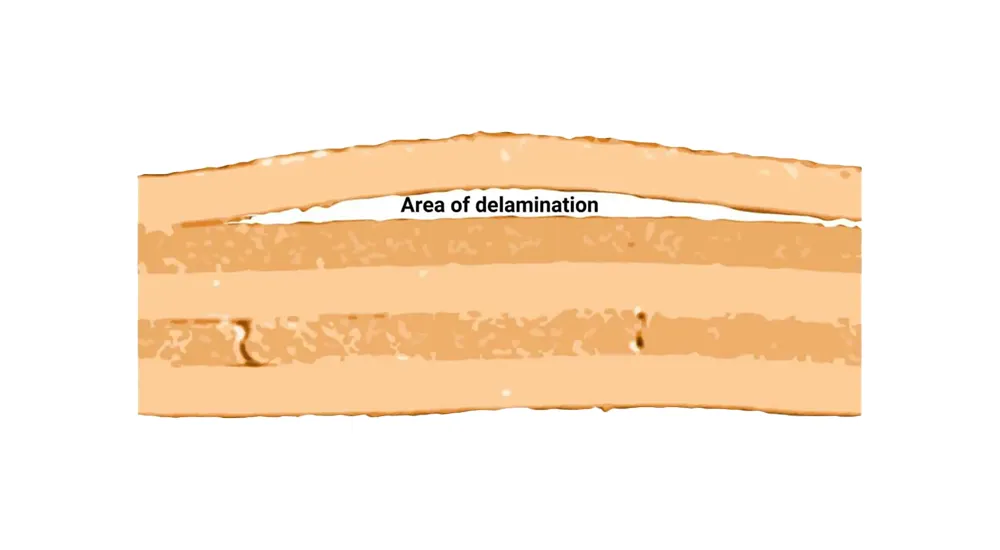
FR4 substrate delamination represents one of the most critical failure modes in multilayer PCB construction. This phenomenon occurs when the bond between copper foil and FR4 substrate weakens, causing visible separation or bubbling. The primary triggers include inadequate surface preparation during manufacturing, contamination of bonding surfaces, or excessive thermal stress during reflow soldering processes.
Moisture absorption into the FR4 substrate creates internal pressure during high-temperature exposure, forcing layers apart. This mechanism becomes particularly problematic in high-density interconnect designs where multiple lamination cycles stress the material beyond its mechanical limits.
Copper Lifting and Trace Damage
PCB copper lifting prevention requires understanding the mechanical forces that cause conductor separation from the substrate. Rapid temperature changes during soldering operations create differential thermal expansion between copper traces and the underlying FR4 material. When these expansion coefficients mismatch significantly, shear forces develop at the interface.
Poor adhesion promoter application or inadequate surface roughening during manufacturing leaves copper traces vulnerable to mechanical stress. Additionally, excessive current density through narrow traces generates localized heating that weakens the copper-to-substrate bond over time.
Via Barrel Cracking and Interconnect Failures
FR4 via barrel cracking occurs when plated through-holes experience mechanical stress that exceeds the copper plating’s tensile strength. This failure mode typically develops during thermal cycling when the FR4 substrate expands and contracts at different rates than the copper plating within the via.
Aspect ratio considerations become critical in thick boards where deep vias require robust plating to maintain electrical continuity. Poor hole wall preparation or inadequate copper thickness distribution creates stress concentration points that initiate crack propagation under repeated thermal loading.
Dielectric Breakdown and Electrical Failures
FR4 dielectric breakdown manifests when the insulating properties of the substrate deteriorate under electrical stress. High voltage applications or inadequate spacing between conductors can create electric field concentrations that exceed the material’s breakdown threshold.
Moisture ingress into the FR4 substrate significantly reduces dielectric strength, creating conductive paths that lead to electrical failures. Temperature elevation during operation further degrades the dielectric properties, accelerating the breakdown process in critical applications.
Thermal Stress and Warping Issues
FR4 thermal stress failures result from dimensional changes during temperature cycling that exceed the material’s mechanical limits. Multilayer constructions with mixed copper distribution create unbalanced thermal expansion that induces board warping and component stress.
Impedance control FR4 boards face additional challenges when thermal expansion affects trace geometry, altering electrical characteristics beyond acceptable tolerances. Glass transition temperature considerations become crucial in applications where operating temperatures approach the FR4’s thermal limits.
Registration and Alignment Problems
Multilayer FR4 registration issues occur when layer-to-layer alignment tolerances exceed design specifications during lamination processes. These problems typically manifest as via-to-pad misalignment or trace registration errors that compromise electrical performance and reliability.
Stack-up variations and material handling procedures significantly influence registration accuracy. Temperature and pressure profiles during lamination directly affect dimensional stability, requiring precise process control to maintain alignment specifications across large panel sizes.

Prevention Strategies and Best Practices
Effective FR4 PCB failure prevention begins with material selection and qualification procedures that ensure substrate consistency and reliability. Proper storage conditions maintain material properties by controlling moisture exposure and temperature fluctuations that can degrade FR4 characteristics before processing.
Manufacturing process optimization focuses on thermal profile management to minimize thermal stress while ensuring adequate reflow conditions for reliable solder joint formation. Surface preparation protocols must establish consistent adhesion promotion between layers and maintain cleanliness standards that prevent contamination-related failures.
Design rule verification ensures that electrical and mechanical specifications remain within FR4 material capabilities. Via design considerations should account for aspect ratios and plating requirements that prevent barrel cracking under operational stresses.
Quality control measures throughout manufacturing processes enable early detection of potential failure modes before they propagate into field failures. Statistical process control and failure analysis feedback loops continuously improve manufacturing capabilities and prevent recurring defect patterns.
Conclusion
Understanding and preventing FR4 PCB failures requires comprehensive knowledge of material properties, manufacturing processes, and failure mechanisms. By implementing proper design practices, maintaining strict process controls, and utilizing advanced manufacturing capabilities, engineers can significantly reduce failure rates and improve product reliability.
The key to successful FR4 PCB manufacturing lies in recognizing potential failure modes early in the design phase and implementing appropriate prevention strategies throughout the manufacturing process. This proactive approach ensures that FR4 PCBs meet performance requirements while maintaining long-term reliability in demanding applications.
Professional FR4 PCB Manufacturing Excellence: Haoyue Electronics
Addressing these complex FR4 PCB failure modes requires advanced manufacturing capabilities and extensive process expertise. At Haoyue Electronics, our comprehensive approach to FR4 PCB manufacturing and assembly incorporates proven failure prevention strategies that ensure consistent product reliability.
Our technical capabilities include precise thermal profile control for lamination processes, advanced surface preparation techniques that optimize layer adhesion, and rigorous quality control systems that detect potential failure modes before shipment. We maintain strict material handling protocols and environmental controls that preserve FR4 substrate properties throughout manufacturing operations.
- Advanced multilayer lamination with registration accuracy better than ±0.05mm
- Controlled impedance manufacturing for high-frequency applications
- Comprehensive thermal stress testing and qualification procedures
- Via design optimization and plating process control
- Statistical process monitoring and failure analysis capabilities
For critical applications requiring exceptional FR4 PCB reliability, our engineering team provides design consultation and manufacturing process optimization that addresses potential failure modes during the development phase. Contact Haoyue Electronics to discuss how our advanced manufacturing capabilities can ensure the reliability and performance of your FR4 PCB requirements.

