The thickness of your flexible PCB directly determines product reliability, manufacturing cost, and design feasibility. Making the wrong choice can result in premature failures, increased production costs, or design constraints that compromise your product’s competitive advantage. This guide provides the technical framework needed to select optimal flexible PCB thickness for any application.
Understanding Flexible PCB Thickness Fundamentals
Material Stack-up Components
Flexible PCB thickness results from multiple material layers working together to provide both electrical functionality and mechanical performance. The primary components include the flexible substrate, conductive copper layers, protective coverlay, and optional stiffener sections.
Substrate Foundation
The flexible substrate serves as the structural foundation while maintaining bend characteristics. Polyimide film represents the industry standard, offering thermal stability from -200°C to +400°C. Standard polyimide thicknesses include 12.5 μm for ultra-thin applications, 25 μm for general-purpose designs, 50 μm for enhanced stability, and 75–125 μm for robust constructions.
Conductive Layers
Copper foil thickness directly impacts both electrical performance and mechanical properties. Common copper weights include 0.5 oz (18 μm) for signal routing, 1 oz (35 μm) for general-purpose applications, and 2 oz (70 μm) for high-current requirements.
Protective Coverlay
Coverlay materials protect conductor patterns while contributing to overall thickness. Typical thicknesses range from 12.5 μm for minimum protection to 75 μm for harsh environments.
Standard Thickness Classifications
The industry recognizes four primary thickness categories. Ultra-thin circuits (25–75 μm) maximize flexibility for space-critical applications like smartphone hinges. Thin circuits (75–150 μm) represent the most common specification, balancing flexibility with manufacturability. Medium circuits (150–250 μm) provide increased mechanical robustness for industrial applications. Thick circuits exceeding 250 μm approach rigid-flex characteristics with maximum durability.
Critical Factors Influencing Thickness Selection
Mechanical Performance Requirements
Bend Radius Calculations
The relationship between thickness and minimum bend radius follows established engineering principles. Industry standards specify minimum bend radius multipliers of 0.1 times thickness for single-layer circuits without coverlay, increasing to 0.25 times thickness for multilayer circuits with coverlay protection.
Dynamic Flexing Considerations
Applications involving repeated bending cycles require careful thickness optimization to prevent material fatigue. Circuits exceeding 100,000 flex cycles demand conservative thickness selections with enhanced safety margins.
Electrical Performance Considerations
Current Carrying Capacity
Conductor thickness determines current handling capability through the relationship between cross-sectional area and allowable current density. Standard calculations assume 1 amp per mil of conductor width for 1 oz copper at 10°C temperature rise.
Signal Integrity Requirements
High-frequency applications require controlled impedance characteristics dependent on conductor geometry and dielectric properties. Thinner substrates may compromise impedance control accuracy while enabling overall thickness reduction.
Environmental and Reliability Factors
Operating temperature ranges, chemical exposure, and mechanical stress conditions significantly influence optimal thickness selection. High-temperature applications may require enhanced substrate thickness for dimensional stability, while aggressive environments necessitate increased coverlay thickness for protection.

Thickness Selection Decision Framework
Systematic Selection Process
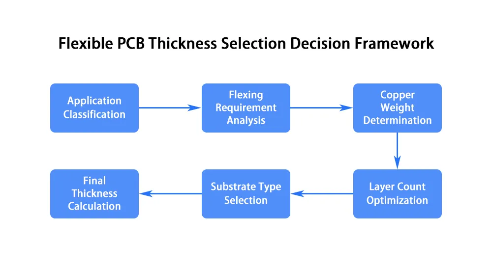
Engineers require a structured approach to navigate the complex interdependencies between application requirements and material specifications. The following six-step framework provides logical progression from initial requirements through final thickness determination.
Step 1: Application Classification
Identify your application category to establish baseline requirements. Consumer electronics typically require 50–100 μm thickness for space optimization. Automotive applications demand 150–300 μm for environmental resistance. Medical devices require 100–200 μm for biocompatibility and sterilization resistance. Aerospace applications range from 75–250 μm balancing weight and reliability. Industrial controls typically specify 125–200 μm for operational reliability.
Step 2: Flexing Requirement Analysis
Document all bending scenarios including static installations, dynamic flexing operations, and multi-axis movement patterns. Static installations allow maximum thickness within space constraints. Occasional flexing requires moderate thickness with safety margins. Dynamic flexing demands minimized thickness optimized for fatigue resistance. Continuous motion applications require ultra-thin construction with enhanced flexibility.
Step 3: Copper Weight Determination
Calculate current carrying requirements for all conductor paths including power distribution and signal routing. Signal routing applications typically use 0.5 oz copper. Low power distribution requires 1 oz copper. Moderate power applications specify 1.5 oz copper. High current applications demand 2 oz copper thickness.
Step 4: Layer Count Optimization
Balance electrical requirements against thickness constraints by optimizing trace routing and layer utilization. Single-layer construction provides minimum thickness with limited routing capability. Double-layer design offers standard thickness with good routing flexibility. Multilayer construction enables complex routing with increased thickness.
Step 5: Substrate Type Selection
Choose substrate materials based on performance requirements and cost constraints. Standard polyimide serves general-purpose applications with proven reliability. Adhesiveless polyimide provides reduced thickness with enhanced flexibility. Liquid crystal polymer offers dimensional stability for specialized applications. Advanced composites address extreme performance requirements.
Step 6: Final Thickness Calculation
Combine all material layers while verifying compliance with mechanical, electrical, and environmental requirements. Include manufacturing tolerances typically ±10% for standard processes and design margins for reliability assurance.
Material Selection and Thickness Optimization
Substrate Material Properties
Standard polyimide films provide excellent thermal stability and chemical resistance while maintaining flexibility across wide temperature ranges. These materials offer proven reliability with established supply chains and competitive pricing. Continuous operating temperature reaches 200°C with glass transition temperature of 360°C.
Adhesiveless constructions eliminate adhesive layers, reducing overall thickness while improving flexibility and thermal performance. These constructions require specialized manufacturing processes but enable significant thickness reductions for space-critical applications.
Conductor Configuration Options
Rolled annealed copper provides optimal flexibility characteristics for dynamic applications compared to electrodeposited alternatives. Alternative conductor technologies including printed silver and printed copper enable ultra-thin constructions while maintaining adequate electrical performance for low-current applications.
Protection System Design
Standard coverlay films provide proven protection with established processing techniques. Photoimageable systems enable selective exposure while maintaining thin profiles but require additional processing steps. Screen-printed protective coatings may enable thickness reductions while providing adequate protection for less demanding applications.
Application-Specific Design Examples
Consumer Electronics Applications
Smartphone and tablet designs drive thickness selection toward the 50–100 μm range while maintaining reliability for typical consumer usage patterns. Single or double-layer constructions with minimum coverlay thickness maximize flexibility while meeting space constraints and cost optimization requirements.
Wearable device applications require conformability to body contours with enhanced flexibility during user movement. Thickness typically ranges from 75–125 μm to balance performance requirements with durability expectations.
Industrial and Automotive Applications
Automotive electronics require environmental resistance with thickness ranging from 150–300 μm. Multiple copper layers support power distribution, while enhanced coverlay systems provide protection against temperature cycling from -40°C to +125°C, vibration resistance, and chemical exposure to automotive fluids.
Medical device applications demand biocompatible materials with specialized material systems and increased thickness for improved handling during assembly and sterilization processes. Thickness selection must consider long-term reliability over the device’s operational lifetime.
| Application Category | Typical Thickness Range | Primary Considerations |
|---|---|---|
| Consumer Electronics | 50–100 μm | Space optimization, cost efficiency |
| Automotive | 150–300 μm | Environmental resistance, durability |
| Medical Devices | 100–200 μm | Biocompatibility, sterilization |
| Aerospace | 75–250 μm | Weight optimization, reliability |
| Industrial Controls | 125–200 μm | Operational reliability, maintenance |
Manufacturing Considerations and Design Guidelines
Process Limitations and Capabilities
Standard manufacturing processes accommodate thickness tolerances of ±10% for circuits exceeding 100 μm thickness. Tighter tolerances require specialized processing with associated cost increases. Ultra-thin circuits below 75 μm total thickness require specialized handling equipment and process controls to prevent damage during fabrication and assembly operations.
Quality control requirements include appropriate thickness measurement systems based on circuit specifications. Non-contact optical systems prevent damage to thin circuits during measurement while providing accurate thickness verification throughout production.
Design for Manufacturing Guidelines
Thin circuits require enhanced handling procedures during fabrication and assembly operations. Component mounting on thin circuits may require stiffener sections or specialized assembly techniques. Assembly process requirements should be considered during initial thickness selection to ensure manufacturing feasibility and cost optimization.
Advanced Design Techniques and Future Trends
Emerging Material Technologies
Next-generation substrate materials including liquid crystal polymers and advanced polyimide formulations enable thickness reductions while maintaining or improving performance characteristics. These materials typically command premium pricing but may enable system-level cost reductions through improved functionality.
Nanocomposite materials incorporating carbon nanotubes or graphene additives provide enhanced electrical and thermal properties while maintaining flexibility characteristics. Commercial availability continues advancing toward broader production readiness.
Manufacturing Process Innovations
Additive manufacturing techniques including screen printing and inkjet printing enable direct conductor pattern formation without traditional etching processes, potentially reducing thickness through elimination of copper foil and adhesive layers.
Roll-to-roll processing capabilities enable high-volume production with improved thickness uniformity compared to sheet-based processing methods. These manufacturing approaches support cost reduction initiatives while enabling enhanced thickness control for demanding applications.
Partner with Haoyue Electronics for Your Flexible PCB Requirements
Selecting optimal flexible PCB thickness requires deep technical expertise combined with advanced manufacturing capabilities. At Haoyue Electronics, our engineering team specializes in helping clients navigate complex design requirements while maintaining cost-effectiveness and manufacturing feasibility.
Our manufacturing facilities support flexible PCB production from ultra-thin 25 μm constructions to robust 500 μm assemblies, with precision thickness control and comprehensive quality verification systems. Whether your application demands consumer electronics optimization or aerospace-grade reliability, our technical team provides the expertise necessary for project success.
Contact our engineering team today to discuss your flexible PCB thickness requirements and discover how our advanced manufacturing capabilities can support your innovative product development.

