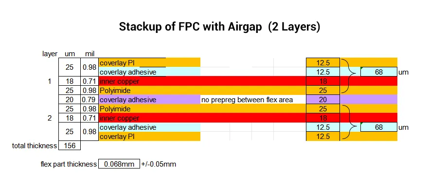
Introduction: Understanding Flexible PCB Stack-up Design
Flexible PCB stack-up represents the layered construction that defines a flexible circuit’s electrical and mechanical characteristics. The stack-up configuration determines signal integrity, bend performance, thermal management, and manufacturing reliability across diverse applications from consumer electronics to aerospace systems.
Unlike rigid PCB designs, flexible circuit stack-ups must accommodate dynamic mechanical stress while maintaining electrical performance. This requirement drives specific material selections, layer arrangements, and construction techniques that distinguish flexible circuits from conventional rigid board technologies. Understanding available stack-up configurations enables engineers to select optimal solutions for specific application requirements.
The selection of appropriate flexible PCB stack-up depends on factors including electrical complexity, mechanical requirements, environmental conditions, and cost constraints. Each configuration offers distinct advantages and limitations that influence overall system performance and manufacturing feasibility.
Single-Layer Flexible PCB Stack-up
Basic Single-Layer Construction
The fundamental single-layer flexible PCB stack-up provides the simplest construction for basic interconnect applications. This configuration consists of a copper conductor layer laminated to a polyimide substrate with protective coverlay applied over the copper traces.
Construction Sequence: The stack-up progresses from bottom to top with polyimide substrate (typically 25 micrometers), adhesive layer (12–15 micrometers), copper conductor (18 micrometers), and protective coverlay (38 micrometers). This arrangement achieves total thickness between 75–100 micrometers while maintaining excellent flexibility characteristics.
Single-layer constructions offer maximum bendability with minimum space requirements, making them ideal for applications requiring tight bend radii or frequent flexing cycles. The simplified construction reduces manufacturing complexity and costs while providing adequate electrical performance for basic signal routing and power distribution.
Application Considerations for Single-Layer Stackups
Single-layer flexible circuits excel in applications requiring simple point-to-point connections, sensor interconnects, and flexible jumpers where electrical complexity remains minimal. The construction supports standard surface mount components and provides reliable electrical continuity through millions of flex cycles when properly designed.
Double-Layer Flexible PCB Stack-up
Symmetrical Double-Layer Configuration
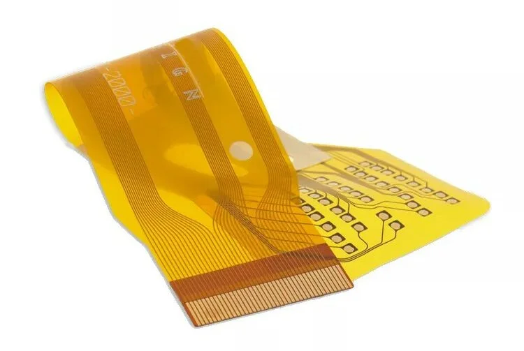
Double-layer flexible PCB stack-ups feature copper conductors on both sides of the polyimide substrate, connected through plated through-holes. This configuration provides enhanced routing capability while maintaining reasonable flexibility characteristics for dynamic applications.
The symmetrical construction places copper layers equidistant from the neutral bending axis, minimizing stress concentration during flexing operations. Coverlay protection on both external surfaces provides comprehensive environmental protection while preserving the essential flexibility characteristics required for dynamic applications.
Electrical Performance Benefits: Double-layer construction enables ground plane implementation, differential signal routing, and improved electromagnetic compatibility compared to single-layer alternatives. The configuration supports controlled impedance design and provides superior signal integrity for high-speed applications requiring reliable electrical performance.
Manufacturing Considerations: Through-hole plating in flexible circuits requires specialized processes to ensure reliable electrical connection while maintaining mechanical integrity. The plating process must accommodate the flexibility requirements without creating stress concentration points that could lead to copper cracking during flexing operations.
Double-Layer with Ground Plane Implementation
Advanced double-layer stack-ups incorporate dedicated ground planes to enhance electrical performance and electromagnetic compatibility. This approach positions signal traces on one layer with a solid or hatched ground plane on the opposite layer, providing controlled impedance characteristics and improved signal integrity.
Ground plane implementation in flexible circuits requires careful copper pattern design to maintain flexibility while providing adequate electrical performance. Hatched or mesh ground patterns offer better mechanical performance compared to solid copper pours, reducing stress concentration during bending operations while maintaining electromagnetic shielding effectiveness.
Multi-Layer Flexible PCB Stack-up Configurations
Four-Layer Flexible Stack-up Design
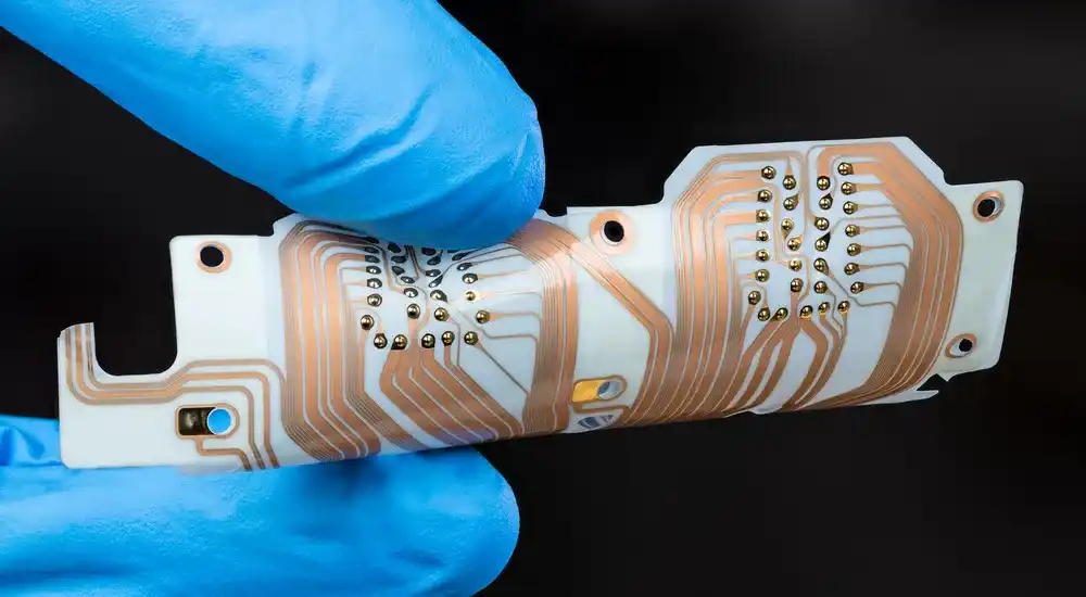
Four-layer flexible PCB stack-ups represent the most common multi-layer configuration, providing enhanced routing density and improved electrical performance while maintaining acceptable flexibility characteristics. The typical arrangement includes two signal layers with dedicated power and ground planes positioned to optimize electromagnetic compatibility.
Layer Arrangement Strategy: The optimal four-layer arrangement positions signal layers between power and ground planes, creating controlled impedance environments for high-speed signals. This configuration minimizes electromagnetic interference while providing clean power distribution throughout the flexible circuit.
Construction complexity increases significantly compared to double-layer designs, requiring multiple lamination cycles and careful process control to maintain layer registration and bond integrity. The additional dielectric layers and copper conductors reduce overall flexibility while improving electrical performance capabilities.
Design Optimization Techniques: Multi-layer flexible designs benefit from copper balancing techniques that distribute copper weight evenly throughout the stack-up. This approach minimizes warpage and internal stress while maintaining manufacturing feasibility within standard process capabilities.
Six-Layer and Higher Configurations
Complex electronic systems often require six-layer or higher flexible PCB stack-ups to accommodate sophisticated signal routing, power distribution, and electromagnetic compatibility requirements. These configurations enable high-density interconnect solutions while maintaining essential flexibility characteristics for dynamic applications.
Advanced Layer Arrangements: Six-layer configurations typically implement signal-ground-power-power-ground-signal arrangements that provide multiple controlled impedance environments and comprehensive electromagnetic shielding. The symmetrical construction minimizes warpage while optimizing electrical performance across diverse signal types.
Higher layer count designs require specialized manufacturing processes including sequential lamination, micro-via technology, and advanced materials to achieve reliable electrical and mechanical performance. The complexity necessitates close collaboration with manufacturing partners to ensure feasibility and cost-effectiveness.
Performance Trade-offs: Increased layer count improves electrical capability while reducing mechanical flexibility and increasing manufacturing costs. Design teams must balance these factors against application requirements to determine optimal stack-up configurations for specific projects.
Rigid-Flex PCB Stack-up Integration
Transition Zone Design Principles
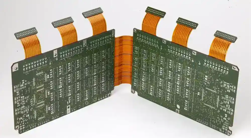
Rigid-flex PCB stack-ups combine flexible circuit sections with rigid board areas, requiring sophisticated design techniques to manage material transitions and stress distribution. The stack-up design must accommodate significant differences in material properties, thermal expansion, and mechanical characteristics between rigid and flexible sections.
Critical Design Elements: Transition zones between rigid and flexible sections require gradual thickness changes to minimize stress concentration. The flexible layers typically continue into rigid areas where they are supported by additional dielectric materials and copper layers that provide mechanical reinforcement.
Successful rigid-flex integration depends on positioning flexible layers appropriately within the overall stack-up construction. Internal placement of flexible circuits provides protection from manufacturing stress and environmental exposure while maintaining electrical continuity between rigid sections.
Layer Count Optimization in Rigid-Flex Design
Rigid-flex stack-ups often feature different layer counts in rigid and flexible sections to optimize performance and cost-effectiveness. The rigid areas may incorporate additional signal layers, power planes, and component mounting areas while flexible sections maintain minimum layer counts necessary for electrical connectivity.
Construction Strategies: The stack-up design coordinates layer requirements between rigid and flexible sections through careful via placement and routing strategies. Buried and blind vias enable electrical connections without compromising the mechanical properties of flexible sections that do not require through-connections.
Manufacturing complexity increases significantly with mixed layer count designs, requiring specialized tooling and process control to maintain registration and electrical performance. The approach enables optimal performance in each section while managing overall cost and manufacturing feasibility.
Adhesiveless Stack-up Alternatives
Adhesiveless Construction Benefits
Adhesiveless flexible PCB stack-ups eliminate traditional structural adhesives through specialized polyimide films with integrated copper bonding. This approach reduces total thickness while improving reliability by removing potential delamination points that can develop in conventional adhesive-based constructions.
Performance Advantages: Adhesiveless constructions provide superior chemical resistance, improved thermal cycling performance, and enhanced mechanical reliability compared to traditional adhesive-based alternatives. The elimination of adhesive layers reduces thickness by 15–20 percent while improving flexibility characteristics.
Manufacturing processes for adhesiveless materials require specialized handling and processing techniques that may increase initial costs. However, the improved reliability and performance characteristics often justify the additional expense for demanding applications requiring superior long-term performance.
Material Selection Considerations
Adhesiveless stack-up design requires careful material selection to ensure compatibility between copper and polyimide components. The specialized materials offer limited supplier options compared to conventional adhesive-based systems, potentially affecting availability and lead times.
Design Implementation
Adhesiveless constructions work particularly well in applications requiring minimal thickness, superior chemical resistance, or enhanced thermal cycling performance. The approach provides significant advantages for aerospace, medical, and automotive applications where reliability requirements justify premium material costs.
Stack-up Selection Guidelines
Application-Specific Design Criteria
Flexible PCB stack-up selection depends on systematic evaluation of electrical requirements, mechanical constraints, environmental conditions, and cost objectives. Each application presents unique challenges that influence optimal stack-up configuration and material selection.
Electrical Requirements Assessment: Signal complexity, impedance control requirements, power distribution needs, and electromagnetic compatibility specifications determine minimum layer count and arrangement. High-speed applications typically require multi-layer constructions with dedicated ground planes, while simple interconnects may utilize single-layer solutions.
Mechanical Performance Evaluation: Bend radius requirements, flex cycle specifications, and installation constraints influence material selection and stack-up configuration. Dynamic applications requiring frequent flexing benefit from thinner constructions with minimal layer counts, while static installations can accommodate more complex multi-layer designs.
Environmental Considerations: Operating temperature ranges, chemical exposure, humidity levels, and mechanical stress determine material requirements and construction techniques. Harsh environments may necessitate adhesiveless constructions or specialized protective systems that influence overall stack-up design.
Cost Optimization Strategies
Stack-up design significantly impacts manufacturing costs through material selection, layer count, and process complexity factors. Understanding these relationships enables design teams to balance performance requirements with economic constraints while maintaining project feasibility.
Manufacturing Efficiency Factors: Standard material thicknesses, proven manufacturing processes, and optimized layer counts reduce production costs while maintaining performance requirements. Early engagement with manufacturing partners provides valuable input regarding cost optimization opportunities and process capabilities.
Panel utilization efficiency and material waste minimization contribute significantly to overall project economics. Stack-up designs that accommodate standard panel sizes and processing capabilities achieve better cost performance compared to specialized constructions requiring custom tooling or processes.
Conclusion: Implementing Optimal Flexible PCB Stack-up Solutions
Flexible PCB stack-up design requires systematic evaluation of electrical, mechanical, and manufacturing requirements to achieve optimal performance and cost-effectiveness. The available configurations range from simple single-layer constructions to complex multi-layer rigid-flex designs that accommodate sophisticated electronic system requirements.
Success in flexible PCB stack-up implementation depends on understanding the capabilities and limitations of each configuration type while maintaining focus on application-specific requirements. Early collaboration with manufacturing partners ensures design feasibility while optimizing performance and cost characteristics.
The continuing evolution of materials, manufacturing processes, and design techniques expands the capabilities of flexible PCB technology while addressing traditional limitations in performance and cost-effectiveness. Staying current with these developments enables design teams to leverage the latest capabilities for competitive advantage in demanding applications.
Accelerate your flexible PCB development with comprehensive design resources and manufacturing support. Professional flexible circuit design requires access to proven stackup configurations, material specifications, and manufacturing guidelines to ensure optimal performance and reliability.
Available Design Resources:
- Flexible PCB stackup design guide with layer configuration templates
- Material selection matrix covering polyimide substrates and copper options
- Stackup thickness calculator for accurate design planning
- Manufacturing capability assessment and design rule verification
- Technical consultation for complex rigid-flex integration projects
Get started with your flexible PCB project today by accessing our comprehensive design resources and connecting with experienced manufacturing partners who understand the unique requirements of flexible circuit technology.
Frequently Asked Questions About Flexible PCB Stack-up
What is the typical thickness of a flexible PCB stackup?
Flexible PCB stackup thickness varies by layer count and construction type. Single-layer flexible circuits typically measure 75–100 micrometers total thickness, while double-layer configurations range from 150–200 micrometers. Multi-layer flexible PCB stackups can reach 300–500 micrometers depending on layer count and material selection. Rigid-flex stackup designs often feature varying thickness between rigid and flexible sections to optimize performance.
How many layers can a flexible PCB stackup have?
Multi-layer flexible PCB stackups commonly range from 2 to 8 layers, with some specialized applications utilizing up to 12 layers. Four-layer flexible stackups represent the most popular multi-layer configuration, offering optimal balance between electrical performance and mechanical flexibility. Six-layer and eight-layer designs provide enhanced routing density for complex applications while maintaining acceptable bend characteristics.
What is the difference between adhesive and adhesiveless flexible PCB stackup?
Adhesive-based flexible PCB stackup construction uses structural adhesives to bond copper foil to polyimide substrates, adding 12–25 micrometers thickness and potential delamination points. Adhesiveless flexible PCB stackup eliminates traditional adhesives through specialized polyimide films with integrated copper bonding, reducing total thickness by 15–20 percent while improving reliability and chemical resistance for demanding applications.
How does rigid-flex stackup design differ from standard flexible PCB?
Rigid-flex stackup design combines flexible circuit sections with rigid PCB areas, requiring sophisticated material transitions and stress management. The flexible layers typically continue into rigid sections where they are supported by additional dielectric materials. Rigid-flex stackup configurations often feature different layer counts between rigid and flexible areas to optimize electrical performance while maintaining essential flexibility characteristics.
What factors determine flexible PCB stackup selection?
Flexible PCB stackup selection depends on electrical requirements including signal complexity and impedance control needs, mechanical constraints such as bend radius and flex cycle specifications, environmental conditions including temperature range and chemical exposure, and cost objectives. Single-layer stackups suit basic interconnects, while multi-layer configurations accommodate complex routing and high-speed signal requirements.

