Introduction: Why Flex PCB Design Needs Specific Guidelines
Key Differences Between Flexible and Rigid PCB Design
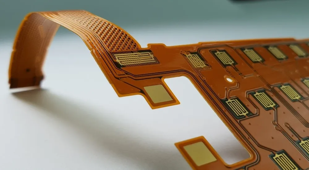
Flexible PCB design fundamentally differs from traditional rigid board design in ways that extend far beyond material selection. While rigid printed circuit boards rely on mechanical stability and predictable material properties, flexible circuits must maintain electrical performance while accommodating mechanical deformation, creating unique engineering challenges that require specialized design approaches.
The primary distinctions between flexible PCB design and rigid board design center on several critical factors:
- Material behavior under stress: Polyimide substrates exhibit different thermal expansion and mechanical properties compared to FR-4 materials.
- Manufacturing process requirements: Specialized lamination, etching, and finishing procedures that differ significantly from standard rigid board fabrication.
- Assembly considerations: Component placement and soldering techniques must accommodate substrate flexibility.
- Reliability factors: Dynamic stress analysis and fatigue life calculations become essential design considerations.
Assembly considerations become more complex as component placement and soldering techniques must accommodate substrate flexibility while maintaining reliable connections. Reliability factors require dynamic stress analysis and fatigue life calculations that are unnecessary for rigid board applications but critical for flexible PCB applications.
Three Core Design Objectives
Successful flexible PCB design must simultaneously achieve three critical objectives that often present competing requirements:
- Reliability: Robust mechanical design that withstands operational stresses throughout the product lifecycle, particularly for dynamic flexing applications where repeated bending cycles create fatigue concerns.
- Manufacturability: Designs that can be produced consistently using available processes and materials while meeting quality standards and cost targets.
- Cost optimization: Balancing performance requirements against material costs, tooling complexity, and yield considerations to deliver economically viable solutions.
These objectives create a design framework where engineering decisions must consider immediate functional requirements alongside long-term reliability and manufacturing constraints. Understanding these fundamental differences establishes the foundation for implementing specific flexible PCB design guidelines that address the unique challenges of flexible circuit development.
Understanding Flex Circuit Types and Application Scenarios
Primary Flex PCB Types and Their Design Impact
The selection of appropriate flex circuit architecture directly impacts design complexity, manufacturing requirements, and performance capabilities. Single-layer flex circuits offer maximum flexibility and minimal thickness profiles, making them ideal for simple interconnections and space-constrained designs. These circuits provide the lowest material and processing costs while delivering adequate performance for basic applications.
Double-layer flexible circuits provide increased routing density while maintaining reasonable flexibility characteristics. The addition of a second conductive layer enables more complex routing patterns and controlled impedance structures, though careful attention to layer symmetry becomes essential for maintaining balanced mechanical properties during bending operations.
Multi-Layer and Rigid-Flex Architectures
Multi-layer flex circuits accommodate high-density routing requirements but significantly increase design complexity and manufacturing costs. Each additional layer reduces flexibility and increases minimum bend radius requirements, necessitating careful evaluation of electrical performance benefits against mechanical limitations. These designs typically serve high-performance applications where routing density justifies the added complexity.
Rigid-flex PCB combinations integrate rigid and flexible sections within a single circuit assembly, eliminating traditional connectors while providing stable mounting areas for components. The transition zones between rigid and flexible sections require specialized design techniques to manage stress concentration and ensure reliable electrical continuity across the interface.
Application Scenarios: Dynamic vs Static Flexing
Understanding the intended flexing application drives fundamental design strategy decisions. Static flexing applications require circuits that can be bent into position during assembly but remain stationary during operation. These designs optimize for installation flexibility while minimizing material costs and complexity, making them suitable for consumer electronics assembly and industrial equipment interconnections.
Dynamic flexing applications involve repeated bending cycles during normal operation, demanding enhanced fatigue resistance and specialized material selection. Examples include printer heads, robotic joints, handheld device hinges, and automotive door systems where continuous movement creates ongoing mechanical stress. These applications require careful evaluation of flex cycle requirements, bending frequency, and environmental conditions to ensure adequate service life.
Bend Radius and Dynamic Flexing Design Rules
Minimum Bend Radius Calculations
Proper bend radius determination forms the foundation of reliable flexible circuit design, with specific requirements varying based on stackup complexity, copper weight, and application demands. Static bend radius guidelines typically specify 6–10 times total stackup thickness for single-layer designs and 10–20 times total thickness for multi-layer constructions. These calculations must include safety margins of 20–30% to accommodate manufacturing variations and ensure consistent performance.
Dynamic bend radius requirements follow more conservative guidelines, with industry standards recommending 20–50 times total stackup thickness minimum for applications involving repeated flexing cycles. The specific multiplier depends on several critical factors:
- Expected cycle counts: Higher cycle requirements demand proportionally larger radii.
- Bending frequency: Rapid cycling creates additional fatigue stress.
- Environmental conditions: Temperature and humidity affect material properties.
- Safety margins: Additional factors for manufacturing variations and long-term reliability.
Copper Weight Impact on Bend Performance
The relationship between copper thickness and achievable bend radius requires careful optimization to balance electrical performance with mechanical flexibility. Standard 18-micrometer electrodeposited copper provides good flexibility for most flexible PCB applications while offering adequate current-carrying capacity for typical circuits. Heavier 35-micrometer copper increases current capacity but significantly enlarges minimum bend radius requirements, making it suitable only for applications where electrical performance justifies the mechanical constraints.
Rolled annealed copper offers superior flexibility and fatigue resistance for dynamic applications but requires specialized processing techniques that may impact availability and cost. This copper type exhibits improved grain structure that resists crack propagation under repeated flexing cycles, making it the preferred choice for high-cycle applications.
Design Strategies for Different Bending Regions
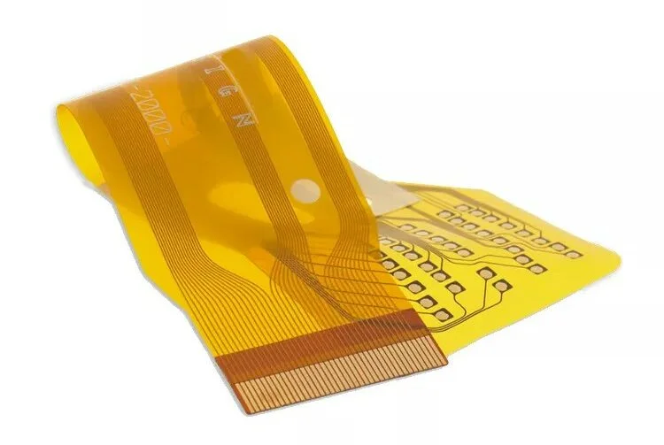
Dynamic bending areas demand simplified routing patterns with traces oriented parallel or perpendicular to the bend axis to minimize stress concentration. Diagonal routing creates uneven stress distribution and should be avoided in critical flex zones. Component placement must exclude all large pads and through-hole features from primary bending areas to prevent stress concentration points that could initiate failures.
Static bend regions accommodate more complex routing patterns while still benefiting from stress relief design techniques. Curved trace routing through transition areas distributes stress more evenly than sharp angular changes, while teardrop connections provide smooth transitions between traces and pads. Width transitions should be gradual rather than abrupt to minimize stress concentration effects.
Stack-Up Planning for Flex PCBs
Fundamental Stackup Design Principles
Effective flexible PCB stack-up design requires balancing electrical performance requirements against mechanical constraints and manufacturing capabilities. Layer symmetry plays a crucial role in preventing unwanted warpage during manufacturing and assembly operations, as asymmetric constructions create inherent bending moments that cause dimensional instability.
Material selection within the stackup affects both electrical and mechanical performance characteristics. Standard polyimide materials provide adequate performance for most applications with continuous operating temperatures up to 150°C and excellent chemical resistance. High-performance polyimides extend temperature capabilities to 200°C while offering enhanced dimensional stability and reduced moisture absorption characteristics for demanding environments.
Neutral Axis Optimization
The positioning of copper layers relative to the bending neutral axis significantly impacts mechanical stress distribution during flexing operations. Copper layers positioned near the neutral plane experience minimal stress, while those positioned away from the center experience proportionally higher stress levels. This relationship becomes critical for multi-layer designs where strategic layer positioning can dramatically improve fatigue resistance.
Thickness control becomes essential for maintaining consistent electrical and mechanical performance across the circuit area. Manufacturing tolerances must be carefully specified to ensure adequate performance margins while maintaining compatibility with connector systems and assembly requirements.
Coverlay vs Flexible Solder Mask Selection
The choice between coverlay and flexible solder mask significantly impacts both performance characteristics and manufacturing costs. Coverlay provides superior mechanical protection and temperature resistance, making it ideal for dynamic applications and harsh environments. However, coverlay requires mechanical registration processes that demand careful tolerance management and increase processing complexity.
Flexible solder mask offers cost effectiveness and design flexibility while maintaining adequate protection for many applications. The liquid application process provides better fine-feature definition capability and simplified processing using standard equipment, though mechanical protection remains limited compared to coverlay alternatives.
Rigid-Flex Transition Zone Management
The interface between rigid and flexible sections represents a critical design area requiring specialized attention to manage the significant stiffness discontinuity. Gradual transitions using tapered stiffener designs or controlled adhesive fillets help distribute mechanical loads over larger areas, reducing stress concentration at the boundary interface.
Layer termination strategy becomes important for managing electrical continuity across the transition while maintaining mechanical integrity. Proper via placement and trace routing through the transition zone ensures reliable signal transmission while minimizing stress concentration effects that could lead to fatigue failures.
Routing and Via Design Guidelines
Trace Routing Optimization for Flexible Circuits
Effective trace routing in flexible PCB design requires techniques that minimize stress concentration while maintaining electrical performance. Trace width selection must balance current-carrying requirements with mechanical stress distribution considerations, as wider traces distribute mechanical loads more effectively but increase local stiffness and reduce routing density.
The orientation of traces relative to bend axes significantly impacts both mechanical reliability and electrical performance. Traces aligned parallel to the bend axis experience minimal stress during flexing operations, while perpendicular orientations distribute stress across the trace width. This relationship becomes particularly important for dynamic applications where stress minimization directly affects fatigue life.
Signal Integrity Considerations
Controlled impedance design in flexible circuits requires accommodation of polyimide dielectric properties and thickness variations that differ from standard FR-4 characteristics. The dielectric constant of polyimide typically ranges from 3.2 to 3.6, requiring adjusted calculations compared to rigid board designs. Cross-hatched reference planes maintain some electromagnetic shielding capability while preserving flexibility characteristics, though careful attention to hatch density and orientation remains necessary.
Differential pair routing demands precise geometric control to maintain impedance matching throughout the flexible section. The spacing between differential pairs must account for crosstalk coupling effects, particularly in multi-layer stackups where interlayer spacing affects electromagnetic coupling behavior.
Via Design and Placement Guidelines
Via implementation in flexible circuits presents unique challenges requiring specialized approaches to maintain mechanical reliability. Through-hole vias create stress concentration points that can initiate crack propagation during flexing operations, making their placement outside primary bend areas essential for reliable operation.
Advanced via technologies such as microvias and blind vias offer alternatives that minimize mechanical discontinuities while providing necessary interconnection capabilities. Microvias provide fine-pitch interconnection with reduced mechanical impact, though they require specialized manufacturing processes that may affect cost and availability. Via-in-pad techniques can provide space-saving benefits while requiring careful consideration of thermal management during assembly operations.
Material and Thickness Considerations in Design Stage
Polyimide Substrate Selection
Material selection for flexible circuits encompasses multiple interdependent factors that affect electrical performance, mechanical reliability, and manufacturing feasibility. Standard polyimide materials provide adequate performance for most applications while offering broad supplier availability and cost-effective solutions. These materials typically support continuous operation up to 150°C with excellent chemical resistance and dimensional stability.
High-performance polyimide options extend temperature capabilities to 200°C while offering enhanced dimensional stability and reduced moisture absorption characteristics. These specialized materials serve demanding applications in aerospace, automotive, and medical device sectors where standard materials prove inadequate, though premium pricing requires justification through performance necessities.
Copper Selection and Treatment
Copper characteristics significantly impact both electrical and mechanical performance in flexible applications. Electrodeposited copper provides excellent adhesion to polyimide substrates while offering uniform thickness control and compatibility with conventional fabrication methods. This copper type delivers adequate flexibility for most static and moderate dynamic applications while maintaining cost-effectiveness.
Rolled annealed copper delivers superior flexibility and fatigue resistance for demanding dynamic applications through optimized grain structure that resists crack propagation. However, this copper type requires modified fabrication techniques and commands premium pricing that must be justified by application requirements.
Critical Design Considerations
A fundamental design consideration involves avoiding the application of standard FR-4 modeling approaches when designing flexible circuits. The material properties, thermal expansion characteristics, and mechanical behavior of polyimide-based flexible materials differ substantially from glass-reinforced epoxy systems, requiring specialized design tools and analysis techniques for accurate performance prediction.
Thickness control strategies must account for manufacturing tolerances while ensuring adequate performance margins for critical applications. Total stackup management affects bend radius calculations and connector compatibility, while layer balance prevents warpage and dimensional instability during processing and assembly operations.
Design for Manufacturability (DFM) for Flex Circuits
Panel Utilization and Cost Optimization
Manufacturing optimization requires careful attention to efficiency factors that directly impact unit costs while maintaining quality standards. Panel layout optimization must balance material utilization efficiency against handling requirements and processing constraints. Dense layouts reduce material waste and tooling costs but may create handling difficulties during manufacturing operations, requiring careful evaluation of trade-offs.
Standard panel sizes and tooling configurations reduce setup costs and lead times while ensuring compatibility with established manufacturing processes. Specialized requirements may justify premium processes when performance necessities demand capabilities beyond standard offerings, though cost implications require careful evaluation against performance benefits.
Manufacturing Process Compatibility
Design features should align with established process capabilities to ensure cost-effective production and reliable quality. Standard manufacturing capabilities support most design requirements while offering predictable costs and delivery schedules. Exotic materials or non-standard geometries may exceed standard capabilities, requiring specialized processes that significantly impact both cost and lead time.
Quality control considerations should include design features that facilitate inspection and testing operations. Clear identification of critical dimensions and performance requirements helps ensure consistent manufacturing results while providing clear acceptance criteria for incoming inspection procedures.
Coverlay Design and Tolerance Management
Coverlay implementation requires precise coordination between design intent and manufacturing capabilities to ensure reliable results. Pad clearance requirements must provide adequate margins for registration tolerance and thermal expansion while maintaining necessary protection and mechanical support. Standard clearance specifications minimize cost while ensuring adequate performance for most applications.
Component accommodation requires sufficient opening sizes for assembly operations while maintaining mechanical integrity around connection areas. Manufacturing tolerance specifications should reflect actual process capabilities rather than theoretical ideals, as overly tight tolerances create unnecessary cost and yield challenges without corresponding performance benefits.
Testing Pads, Connectors, and Assembly Considerations
Pad Reinforcement Design for Flexible Circuits
Standard pad designs often prove inadequate for flexible circuit applications, requiring specialized reinforcement techniques to prevent trace lifting and ensure reliable connections during assembly and operation. Anchor pad configurations extend traditional pad designs to distribute mechanical loads over larger areas, reducing stress concentration at connection points.
Flying lead structures provide strain relief through controlled trace geometry that accommodates connector insertion forces and thermal expansion effects. These designs help prevent trace peeling during handling operations while maintaining electrical connectivity and mechanical integrity under operational stresses.
Assembly Process Compatibility
Surface mount technology application to flexible circuits requires specialized techniques that accommodate substrate flexibility while maintaining assembly line compatibility. Temporary support systems using rigid carriers provide mechanical stability during component placement and soldering operations, ensuring consistent assembly results with standard equipment.
Hot-bar soldering techniques offer precise temperature and pressure control for reliable attachment of flexible circuits to connectors and rigid assemblies. These processes require specific pad designs and material considerations to ensure reliable solder joint formation while preventing substrate damage from excessive heat or pressure.
Connector Interface Design
Zero insertion force (ZIF) connector applications require precise thickness specifications and controlled stackup tolerances to ensure proper engagement and reliable electrical connection. Contact area design must optimize pad geometry for consistent electrical performance while accommodating the mechanical requirements of the connector system.
FPC connector considerations include compatibility with standard connector specifications and thickness tolerance requirements that ensure proper mechanical fit. Surface finish selection affects both electrical performance and mechanical durability, requiring evaluation of contact resistance, solderability, and wear characteristics for the intended application.
Common Design Mistakes to Avoid
Critical Design Errors in Flexible Circuit Development
The most serious design errors typically result from applying rigid board design practices without considering the unique requirements of flexible materials and applications. Common critical mistakes include:
- Via placement in bend areas: Creates stress concentration points leading to premature failure through crack propagation.
- Component pads within flex zones: Large pads and through-hole features cause mechanical stress concentration.
- Inappropriate material selection: Standard materials inadequate for dynamic applications or environmental conditions.
- Insufficient stress relief: Sharp geometry changes and abrupt transitions create failure initiation points.
Material and structure selection errors often stem from inadequate consideration of dynamic flexing requirements or environmental conditions. Standard materials may prove inadequate for repeated bending applications, while inappropriate copper selection can significantly limit fatigue life or create processing difficulties that affect yield and cost.
Manufacturing and Assembly Mistakes
Tolerance and clearance errors frequently create assembly difficulties and reliability issues that could be avoided through proper design coordination. Insufficient coverlay window clearances may interfere with assembly operations, while inadequate spacing around components creates handling difficulties during manufacturing and assembly processes.
Design tool compatibility issues arise when engineers attempt to use rigid board design software for flexible circuit applications. Standard simulation tools may provide inaccurate results for flexible circuit behavior, while conventional design rule checks may not address the unique requirements of flexible materials and applications.
Documentation and Communication Failures
Inadequate documentation and communication with manufacturing partners often results in misinterpretation of design intent and suboptimal manufacturing processes. Complete specification of materials, stackup configurations, bend requirements, and assembly considerations ensures consistent manufacturing results and facilitates supplier qualification processes.
Quality standards must include specific acceptance criteria for both electrical and mechanical performance parameters. Clear identification of critical dimensions and tolerance requirements helps prevent manufacturing issues while providing objective criteria for incoming inspection and quality control procedures.
Conclusion and Design Collaboration Tips
Design Priority Framework
Successful flexible PCB design implementation requires systematic prioritization of competing objectives based on application requirements and risk assessment. Flexing reliability typically takes precedence over other considerations, as mechanical failures often result in complete circuit failure and difficult field repairs. Electrical performance requirements must be met within mechanical constraints, while cost optimization should be pursued within boundaries established by reliability and performance specifications.
Design validation through prototyping and testing provides essential feedback for optimizing final designs before committing to production tooling. Mechanical testing under representative conditions helps validate bend radius calculations and fatigue life predictions, while electrical testing confirms performance under operational conditions and environmental stresses.
Manufacturing Partnership Strategy
Early collaboration with manufacturing partners should begin during the conceptual design phase to ensure compatibility with available processes and materials. Experienced manufacturers can provide valuable guidance on material selection, stackup optimization, and design for manufacturability considerations that significantly impact both cost and reliability outcomes.
Regular design reviews incorporating manufacturing feedback help identify potential issues before they become costly problems requiring design iterations. These reviews should address material availability, process compatibility, yield considerations, and cost optimization opportunities while maintaining specified performance requirements.
The complexity of flexible circuit design often justifies investment in specialized design tools and analysis capabilities that provide more accurate modeling of flexible circuit behavior. These tools facilitate optimization of electrical and mechanical performance parameters while reducing the risk of costly design errors and manufacturing difficulties.
Partnership with Haoyue Electronics
Need support for your complex flex PCB design? Haoyue Electronics offers expert design for manufacturability feedback and stack-up planning tailored to your specific application requirements. Our experienced engineering team collaborates with clients throughout the development process, from initial concept through high-volume production, ensuring optimal balance between performance, reliability, and cost-effectiveness. Contact us to discuss how our proven flexible PCB design expertise can accelerate your development timeline while minimizing technical risks and optimizing manufacturing outcomes for your next innovative product.

