Understanding Double Layer PCB Stackup Architecture
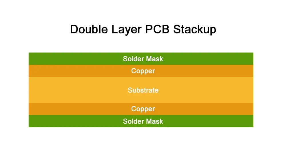
A double layer PCB stackup features two conductive copper layers separated by a dielectric substrate, most commonly made from FR4 material. This configuration supports component placement on both sides of the board and provides essential via connections between layers. It forms the core structure for signal routing, power distribution, and grounding in a wide range of electronic circuits.
The basic construction involves a solid dielectric core with copper foil laminated on both surfaces. Unlike multilayer PCBs that use prepreg layers for interlayer bonding, double layer boards rely primarily on the core thickness to define the board’s overall dimensions. This streamlined architecture allows for faster fabrication, simpler processing, and lower production costs.
Core Materials and Specifications
The dielectric core in a double layer PCB stackup typically consists of FR4, a glass-reinforced epoxy laminate, with standard thicknesses ranging from 0.4 mm to 3.2 mm. The material’s electrical properties—particularly its dielectric constant (Dk), which typically falls between 4.2 and 4.8 for standard FR4—directly influence signal performance.
For applications demanding higher performance, alternative materials such as Rogers RO4000 series or ISOLA high-frequency laminates may be selected to provide lower Dk values, improved thermal stability, or enhanced high-speed signal integrity.

Primary Configuration Types
1. Signal-Signal Configuration
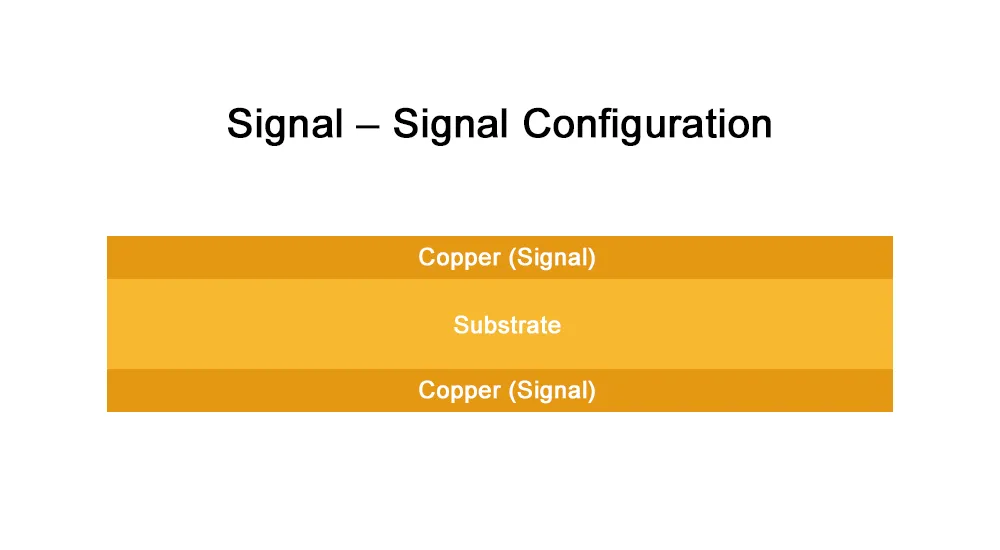
The signal-signal configuration is the most common double layer PCB stackup, where both copper layers are used for routing signal traces. This setup maximizes routing density and allows for component placement, power delivery, and ground connections on both sides of the board.
Key benefits of the signal-signal configuration include:
- High component density on both board surfaces
- Flexible routing for complex circuit layouts
- Cost-effective for low to moderate frequency designs
- Suitable for mixed-signal applications with proper isolation
However, this configuration may present challenges in high-frequency applications due to limited ground plane continuity, which can lead to signal integrity issues and increased EMI.

2. Signal-Ground Configuration
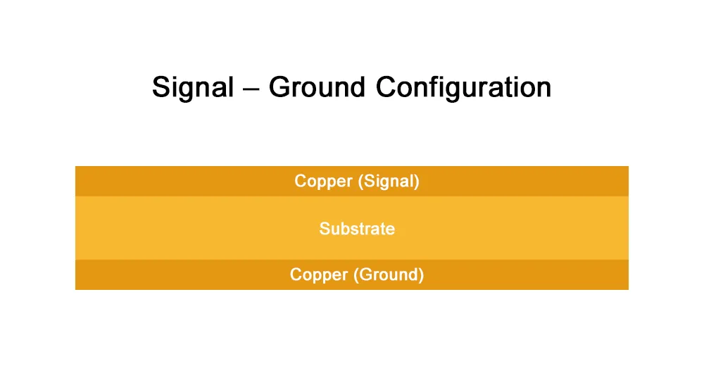
In the signal-ground configuration, one layer is dedicated solely to ground while the other is used for signal routing and component placement. This structure enhances signal integrity and provides better EMI shielding, making it ideal for high-speed and noise-sensitive designs.
Advantages of the signal-ground configuration include:
- Improved signal integrity with a continuous ground reference
- Better impedance control for critical signal paths
- Enhanced EMI shielding and reduced crosstalk
- Simplified return path for high-speed signals
The main drawback is reduced component density, as components can only be placed on the signal layer, potentially increasing the overall board size.
Design Considerations and Best Practices
Impedance Control Implementation
Controlled impedance in double layer PCB stackup design requires careful control of trace width, dielectric thickness, and copper weight. For single-ended signals, impedance is influenced by the spacing between traces and their proximity to the ground plane. In differential pair routing, consistent trace width and uniform spacing are essential to maintain signal integrity and minimize skew and reflection.
Via Design and Placement
Through-hole vias provide essential electrical connections between the top and bottom layers. To ensure reliable performance and manufacturability, via dimensions must balance electrical requirements and fabrication limits. Standard via diameters range from 0.1 mm to 0.8 mm, with aspect ratios typically kept below 8:1.
Thermal Management Strategies
Effective thermal management in double layer PCBs involves the use of copper pours, thermal vias, and dedicated heat-spreading areas. Connecting high-power components to large copper zones enhances heat dissipation. For demanding thermal conditions, designers may consider using heavier copper weights and applying thermal interface materials to maintain temperature stability.
Application Domains and Use Cases
Consumer Electronics and IoT Devices
Double layer PCB stackups are widely used in consumer electronics such as smart home devices, wearable tech, and IoT sensors. Their cost efficiency and sufficient performance make them ideal for high-volume manufacturing and compact product designs.
LED Lighting Systems
LED driver boards and lighting control systems often rely on double layer PCBs for both power delivery and thermal management. This configuration supports high current loads and allows for proper spacing of heat-dissipating components.
Industrial Control Systems
In factory automation and industrial environments, double layer PCBs are commonly used in sensor modules, interface boards, and communication controllers. Their mechanical stability and straightforward manufacturing make them suitable for demanding, high-reliability applications.
Performance Characteristics and Limitations
| Aspect | Advantage | Limitation |
|---|---|---|
| Cost | 30-50% lower than 4-layer boards | Higher than single-layer alternatives |
| Signal Integrity | Adequate for <500MHz applications | Limited high-frequency performance |
| Component Density | Supports both-side placement | Lower than multilayer alternatives |
| EMI Shielding | Improved over single-layer | Insufficient for sensitive applications |
| Manufacturing | Standard processes, fast turnaround | Limited stackup options |
Frequency Response Considerations
Double layer PCB stackups are best suited for applications operating below 500 MHz. Beyond this range, maintaining signal integrity becomes increasingly difficult due to factors like crosstalk, EMI, and impedance discontinuities. For high-speed digital circuits, a minimum of four layers is typically required to ensure controlled impedance and adequate shielding.
Power Distribution Networks
Effective power distribution in double layer PCBs requires careful routing strategies, as there are no dedicated power planes. Designers must use wide traces and well-placed ground pours to minimize voltage drop and noise. For high-current applications, increasing copper thickness from the standard 1 oz to 2 oz or 3 oz can improve power stability and thermal performance.
Manufacturing Excellence and Quality Considerations
Fabrication Process Optimization
Double layer PCB stackup manufacturing involves proven processes including drilling, plating, etching, and solder mask application. The simplified layer structure reduces manufacturing complexity while maintaining high yield rates. Standard manufacturing tolerances accommodate most design requirements without specialized processing.
Quality Assurance Protocols
Comprehensive testing protocols for double layer PCB stackup include electrical continuity verification, insulation resistance testing, and dimensional inspection. Advanced testing may incorporate impedance measurement and thermal cycling validation for critical applications.
Future Trends and Technology Evolution
The evolution of double layer PCB stackup continues with advanced materials development, including low-loss dielectrics and enhanced thermal management solutions. Flexible-rigid hybrid constructions and embedded component technologies represent emerging opportunities for this fundamental PCB architecture.
Integration with Industry 4.0 manufacturing principles enables real-time quality monitoring and process optimization, further enhancing the value proposition of double layer PCB stackup for diverse applications.
Partner with Haoyue Electronics for Expert PCB Solutions
At Haoyue Electronics, we specialize in precision manufacturing and assembly of double layer PCB stackup configurations tailored to your specific requirements. Our experienced engineering team provides comprehensive design support, from initial concept through volume production, ensuring optimal performance and reliability for your electronic products.
With state-of-the-art manufacturing facilities and rigorous quality control processes, we deliver consistently high-quality double layer PCBs that meet the demanding requirements of modern electronics. Contact our technical team today to discuss how our expertise in double layer PCB stackup can accelerate your product development and manufacturing goals.
FAQ
1. What is a double layer PCB stackup?
A double layer PCB stackup consists of two conductive copper layers separated by a dielectric substrate, usually made of FR4 material. This structure allows component placement on both sides of the board and enables more complex routing compared to single-layer PCBs.
2. What are the common applications of double layer PCBs?
Double layer PCBs are widely used in consumer electronics, IoT devices, LED lighting systems, and industrial control equipment. Their balance of cost-effectiveness and reliable performance makes them suitable for volume production in diverse industries.
3. How does a signal-ground configuration differ from a signal-signal configuration?
In a signal-ground configuration, one copper layer is dedicated as a continuous ground plane to improve signal integrity and EMI shielding, while the other is used for signal routing. In contrast, the signal-signal configuration uses both layers primarily for routing signals, allowing higher component density but potentially less EMI control.
4. What are key design considerations for double layer PCB stackups?
Important design factors include impedance control through trace geometry and dielectric thickness, optimal via sizing and placement, and effective thermal management using copper pours and thermal vias to dissipate heat from high-power components.
5. Can double layer PCBs be used for high-frequency applications?
Double layer PCBs generally perform well for frequencies below 500 MHz. For higher-frequency or high-speed digital circuits, multilayer PCBs (typically four layers or more) are recommended to maintain signal integrity and reduce electromagnetic interference.
6. How does manufacturing quality assurance work for double layer PCBs?
Quality assurance includes electrical continuity testing, insulation resistance checks, dimensional inspections, and sometimes advanced methods like impedance measurement and thermal cycling. These ensure the PCB meets design specifications and reliability standards.

