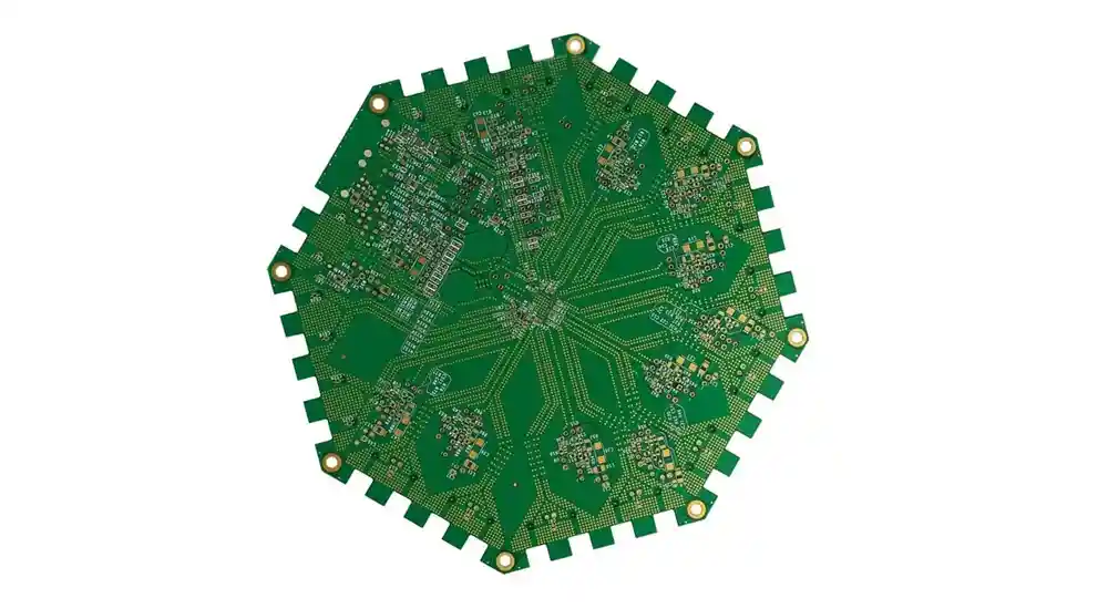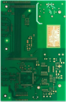
This comprehensive guide delves into essential double layer PCB design strategies, equipping engineers with the knowledge to create reliable, cost-effective solutions that meet the growing demands of high-speed digital environments.
Understanding Double Layer PCB Fundamentals
Layer Configuration and Structure
A Double Layer PCB Design consists of two conductive copper layers separated by an insulating dielectric substrate, commonly made from FR4 material. In a double-sided printed circuit board, conductive traces are laid out on both the front and back of the substrate. These two layers are interconnected through metallized vias, creating an efficient electrical pathway. This configuration offers greater routing flexibility compared to single-layer designs while maintaining cost efficiency when compared to more complex multilayer alternatives.
The standard thickness for double layer PCBs typically ranges from 1.6mm to 2.0mm, with copper weights generally between 0.5oz and 2oz per layer. Understanding these physical characteristics is crucial for achieving effective impedance control and ensuring the mechanical reliability of the board.
Design Considerations for Signal Integrity
As digital switching speeds continue to increase, signal integrity becomes an ever-more critical factor in Double Layer PCB Design. To ensure optimal performance, designers must focus on maintaining signal integrity in their layouts, especially for high-speed circuits. One key consideration is achieving controlled impedance traces. In double layer PCB designs, consistent impedance is essential and requires precise calculation of trace geometry, dielectric thickness, and the spacing to reference planes to prevent signal degradation.
Strategic Component Placement Techniques
Functional Grouping and Thermal Management
Effective component placement is the foundation of successful Double Layer PCB Design. The component placement stage of your PCB layout is both an art and a science, requiring strategic consideration of the available space on the board. Priority should be given to placing essential components first, followed by large processors and critical integrated circuits.
Grouping components based on their functional relationships helps minimize signal path lengths and reduces electromagnetic interference. Analog and digital sections should be separated to prevent noise coupling, while high-power components require careful placement in well-ventilated areas to address thermal management concerns.
Design for Assembly Optimization
Component placement must also consider the assembly process and inspection requirements. Avoid placing components near the edges of the PCB or in locations that complicate automated assembly. Following standard spacing guidelines for pick-and-place machines helps minimize assembly errors, reducing manufacturing costs and improving yield rates.
Advanced Routing Strategies
Orthogonal Routing Implementation
Double layer boards greatly benefit from orthogonal routing strategies, which minimize crosstalk and signal interference. In this approach, traces are routed in perpendicular directions—such as using the top layer for vertical routing and the bottom layer for horizontal routing. This technique helps prevent parallel signal paths on adjacent layers, which could lead to coupling issues.
When implementing orthogonal routing, it is crucial to maintain consistent trace widths and avoid sharp 90-degree angles. Instead, using 45-degree chamfers or curved transitions can minimize signal reflections and reduce electromagnetic radiation, ensuring better signal integrity in Double Layer PCB Designs.
Controlled Impedance Considerations
For high-speed signals requiring impedance control, Double Layer PCB Design presents unique challenges. Achieving the correct impedance on a standard PCB thickness for single-ended signals can be difficult. Engineers must carefully balance trace width, dielectric thickness, and the proximity of reference planes to meet the target impedance values.
Critical impedance parameters for double layer designs include:
| Signal Type | Target Impedance | Typical Trace Width | Design Considerations |
|---|---|---|---|
| Single-ended | 50Ω ± 10% | 0.1-0.3mm | Requires ground reference |
| Differential pairs | 100Ω ± 10% | 0.08-0.15mm | Tight coupling required |
| Clock signals | 50Ω ± 5% | Calculated per spec | Length matching critical |
Power Distribution and Ground Plane Strategy
Effective Power Delivery Networks
In Double Layer PCB Design, it is crucial to balance power distribution requirements with available routing resources. To minimize noise coupling, high-power and low-power planes should be kept separate. Sensitive analog circuits benefit from dedicated ground planes that are isolated from noisy digital sections, ensuring better signal integrity.
By implementing dedicated ground planes on one layer and using the opposite layer for signal routing and power distribution, you can achieve optimal noise performance. Strategic via placement creates multiple current return paths, reducing ground impedance and improving the overall performance of the Double Layer PCB Design.
Via Design and Placement Optimization
Via selection plays a significant role in both the electrical performance and manufacturing costs of Double Layer PCB Designs. Through-hole vias are typically the most cost-effective option. To reduce manufacturing costs, choose standard pad sizes over oversized ones. The standard via specifications for double layer designs typically include a 0.2mm drill diameter with a 0.4mm pad size, ensuring reliable connections while maintaining cost efficiency.
When connecting high-current paths between layers, multiple vias should be used in parallel to effectively distribute current and heat. For high-power applications, use multiple vias to handle higher currents without causing excessive temperature rise. Placing vias in an array or grid pattern helps evenly distribute current and heat, improving the thermal and electrical performance of the PCB.

Design for Manufacturability Excellence
Cost Optimization Strategies
Manufacturing cost reduction begins with intelligent design choices that align with standard fabrication processes. Efficient material usage, minimizing layer counts, and designing for manufacturability (DFM) all help reduce costs. Key cost optimization strategies include:
Using standard materials such as FR4 with common dielectric constants and copper weights reduces tooling requirements and material costs. Avoiding exotic materials and non-standard thicknesses, unless absolutely necessary, helps maintain compatibility with high-volume manufacturing processes, ensuring cost-effectiveness in Double Layer PCB Design.
Optimizing trace width strikes a balance between electrical requirements and manufacturing capabilities. It is important to keep trace widths within reasonable limits for a cost-effective design while ensuring they meet impedance requirements to maintain connectivity between components. Minimum trace widths should align with manufacturer capabilities, providing adequate current-carrying capacity without unnecessary complexity.
Manufacturing Process Considerations
Design for manufacturability principles significantly impact production yield and overall costs. Did you know that up to 70% of PCB manufacturing issues stem from design flaws? Mastering PCB Design for Manufacturing (DFM) is critical for preventing these issues and optimizing the production process, especially in Double Layer PCB Design.
Critical DFM guidelines for double layer designs include maintaining adequate clearances between features, using standard drill sizes, and avoiding overly complex routing patterns. Proper component orientation should facilitate automated assembly processes and provide adequate access for inspection and testing, streamlining the overall manufacturing workflow.
Signal Integrity Validation and Testing
Pre-production Verification Methods
Signal integrity verification requires systematic analysis of critical timing paths and impedance characteristics. Impedance control can be verified after the PCB is manufactured by using test coupons (a test coupon is a PCB used to test the quality of the PCB fabrication process. Test coupons are fabricated on the same panel as the PCBs, typically at the edges, ensuring proper layer alignment, electrical connectivity, and cross-section).
Time-domain reflectometry testing validates impedance continuity across the entire signal path, identifying discontinuities that could impact performance. This verification process should include both single-ended and differential signal paths where applicable, ensuring optimal signal integrity in Double Layer PCB Design.
EMI and EMC Considerations
Electromagnetic compatibility becomes increasingly important as operating frequencies rise and product certification requirements tighten. EMI and electromagnetic compatibility (EMC) can be managed with direct signal paths and by avoiding right-angle turns in traces. Ground planes and strategic shielding around sensitive analog sections also contribute to effective EMI and EMC control.
Effective EMI mitigation techniques include implementing continuous ground reference planes, minimizing loop areas in current return paths, and using proper trace termination techniques for high-speed signals. These practices are essential in ensuring robust performance in Double Layer PCB Designs, particularly in high-frequency applications.

Material Selection and Stack-up Design
Dielectric Material Optimization
Material selection significantly influences both electrical performance and manufacturing costs in Double Layer PCB Design. Standard FR4 materials offer adequate performance for most applications while maintaining cost-effectiveness. FR-4 Glass Epoxy is the most common material, while CEM-1 Paper Epoxy is a low-cost option, and materials like Rogers and Arlon are used for high-frequency boards.
For high-frequency applications requiring superior signal integrity, low-loss materials such as Rogers or Arlon substrates may justify their additional cost through improved performance characteristics. These materials are often selected for double layer PCB designs to ensure optimal signal quality and reliability in demanding environments.
Surface Finish Selection
Surface finish selection impacts both solderability and long-term reliability in Double Layer PCB Design. To reduce PCB costs, HASL and OSP are optimal choices. Cost-effective options include Hot Air Solder Leveling (HASL) for general applications and Organic Solderability Preservative (OSP) for fine-pitch components.
For applications requiring superior flatness or multiple reflow cycles, Electroless Nickel Immersion Gold (ENIG) provides enhanced reliability, despite higher material costs, making it ideal for high-performance double layer PCB designs in critical applications.
Partner with Professional PCB Manufacturing Excellence
Successful double layer PCB design requires both technical expertise and reliable manufacturing partnerships. At Haoyue Electronics, our two decades of industry experience in PCB manufacturing and assembly enable us to support your double layer PCB projects from initial design consultation through high-volume production.
Our comprehensive design for manufacturability review process identifies potential issues early in the development cycle, reducing time-to-market while optimizing manufacturing costs. Whether you require prototype development, design optimization consultation, or full-scale production services, our engineering team provides the technical support necessary to ensure your double layer PCB designs meet both performance requirements and manufacturing objectives.
Contact Haoyue Electronics today to discuss how our proven manufacturing capabilities and design expertise can accelerate your next double layer PCB project while maintaining the highest quality standards.
FAQ
1. What are the key considerations when designing a Double Layer PCB?
When designing a Double Layer PCB, key considerations include proper component placement, signal integrity, impedance control, and effective power distribution. For optimal signal integrity, it’s crucial to implement controlled impedance traces and use appropriate materials, such as FR4 for standard applications or low-loss materials like Rogers for high-frequency designs.
Additionally, understanding the mechanical constraints and ensuring that components are placed efficiently to minimize noise and reduce electromagnetic interference are essential for a successful design.
2. How can I ensure the signal integrity of my Double Layer PCB Design?
Signal integrity in Double Layer PCB Design can be ensured by focusing on trace geometry, dielectric thickness, and proper grounding. Techniques like orthogonal routing, where traces are routed in perpendicular directions, minimize signal interference and crosstalk.
It’s also essential to verify impedance continuity through testing methods like time-domain reflectometry. Using materials optimized for high-frequency signals and ensuring proper layer stacking and reference planes are critical for maintaining signal integrity.
3. What factors should I consider when choosing a manufacturer for my Double Layer PCB project?
When selecting a manufacturer for your Double Layer PCB project, consider their expertise in high-volume production, design for manufacturability (DFM) processes, and ability to meet your specific design requirements. Ensure they offer comprehensive design support, including prototyping, optimization consultations, and full-scale production services.
A reliable manufacturer will also provide robust testing procedures to ensure the quality and performance of the finished product. Experience in your industry and adherence to quality standards is also vital for successful project completion.
Related Posts
Single Layer PCB Design | Expert Insights for Reliable Performance
Multilayer PCB Design | Key Considerations and Best Practices
Rigid-Flex PCB Design Guideline | Engineering Excellence Through Strategic Layout and Manufacturing
Comprehensive Guidelines for Flexible PCB Design by Haoyue Electronics
Complete HDI PCB Design Guide | BGA Pitch from 1.0mm to 0.4mm
Metal Core PCB Design Guidelines for Power Electronics & LEDs

