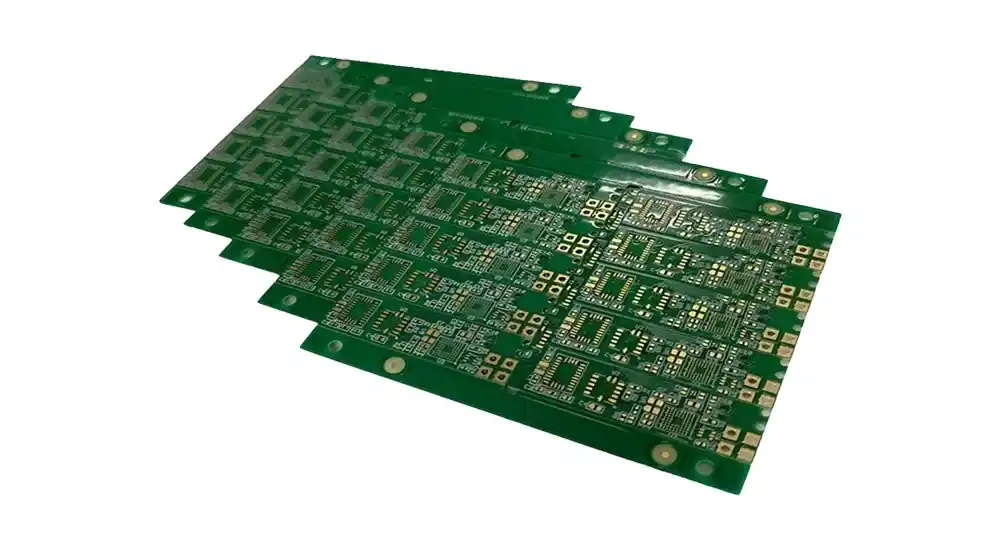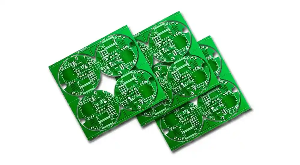
The pricing of double layer PCBs goes beyond raw material expenses to include design requirements, fabrication processes, and production scale. Advances in PCB manufacturing automation have contributed to a 5-10% reduction in unit costs for standard processes in 2025, while online quoting tools have simplified cost estimation. By gaining insight into these interconnected cost factors, organizations can make informed decisions to optimize both the performance and cost-effectiveness of their double layer PCB projects.
Material Selection and Substrate Cost Factors
Base Material Impact on Pricing
The choice of substrate material is one of the most significant cost drivers in double layer PCB manufacturing. Common materials such as FR-4 offer a cost-effective solution, while specialized substrates like Rogers or ceramic cater to high-frequency or high-reliability applications and come at a premium. Typically, substrate material accounts for around 15% of the total cost in mass PCB production.
FR-4 Material Characteristics and Costs: FR-4 remains the most widely used substrate due to its versatile properties and affordability. It provides excellent value and is sufficient for most standard applications operating at low to medium frequencies. FR-4 features high dielectric strength, lightweight construction, robust mechanical strength, and moisture resistance, making it suitable for a broad range of general electronics.
High-Performance Materials for Specialized Applications: For applications demanding superior electrical performance, Rogers substrates excel in high-frequency scenarios thanks to their lower dielectric constant, reduced signal loss, and enhanced thermal stability compared to FR-4. However, Rogers materials are significantly more expensive, reflecting their design focus on high-frequency and high-reliability environments, whereas FR-4 emphasizes cost-effectiveness.
Material Performance Comparison
| Material Type | Dielectric Constant | Cost Premium | Primary Applications |
|---|---|---|---|
| Standard FR-4 | ~4.5 | Baseline | General electronics, consumer products |
| High-Tg FR-4 | ~4.5 | +10-20% | Automotive, industrial applications |
| Rogers 4350B | ~3.48 | +200-400% | RF/microwave, high-frequency circuits |
| Rogers 4003C | ~3.38 | +300-500% | Aerospace, defense, millimeter-wave |
Copper Thickness Considerations
Copper thickness plays a critical role in both material costs and manufacturing complexity. The standard copper thickness of 1 ounce (35 micrometers) is typically included in base pricing. However, opting for thicker copper layers, such as 2 ounces, can increase costs by approximately 50% to 100% compared to the standard. Thicker copper not only raises material expenses but may also require more complex manufacturing processes to handle the increased copper weight.

Design Complexity and Manufacturing Requirements
Board Size and Panel Utilization
Physical board dimensions directly impact material consumption and manufacturing efficiency. PCB costs calculated on an area basis multiply the board’s surface area by a unit price influenced by factors such as layer count, material choice, and fabrication processes. Larger boards naturally require more raw materials and occupy greater space during production.
Optimizing panel utilization is critical for cost reduction. High-volume production benefits from economies of scale, often achieving cost savings between 20% and 50% or more compared to low-volume runs. Manufacturers can nest multiple smaller circuits on a single panel, spreading fixed setup costs across more units and thus lowering per-unit expenses.
Trace Width and Spacing Requirements
The required precision for trace width and spacing significantly affects manufacturing complexity and cost. Fine-pitch designs demand advanced manufacturing equipment and tighter process control, which can increase unit prices. Standard trace widths and spacing generally fall within typical manufacturer capabilities without added charges, whereas ultra-fine pitch requirements often incur premium fees.
Design Guidelines for Cost Management:
- Standard trace widths: 0.1 mm (4 mils) and above
- Standard spacing: 0.1 mm (4 mils) and above
- Via sizes: minimum finished hole diameter of 0.2 mm (8 mils)
- Aspect ratios: maximum of 8:1 for standard processing
Drilling and Via Requirements
The number and complexity of drilled holes have a significant impact on manufacturing costs and cycle times. A higher hole count typically increases PCB fabrication expenses. Standard through-hole drilling usually adds minimal extra cost, while specialized processes such as microvias or laser-drilled holes can substantially raise costs.
Additional processes like via filling and plugging add approximately $10 to $50 per panel, while fine-pitch drilling for microvias and HDI boards may incur extra charges ranging from $5 to $20 per panel. The aspect ratio—calculated as board thickness divided by drill diameter—also influences manufacturability and pricing, with higher ratios requiring more specialized equipment and processes.
Production Volume and Process Variables
Volume-Based Pricing Structures
Production quantity is one of the most influential factors affecting per-unit costs for double layer PCBs. Low-volume orders (5-10 units) typically have higher per-unit prices due to setup and tooling fees, while high-volume production reduces costs by spreading fixed expenses over more units. Pricing generally shows a steep decline at low volumes before stabilizing as production quantities increase.
Typical Volume Pricing Brackets:
- Prototype quantities (1-10 units): Highest per-unit cost due to full setup allocation
- Small production runs (11-100 units): 30-50% reduction from prototype pricing
- Medium volume (101-1,000 units): Additional 20-30% cost reduction
- High volume (1,000+ units): Pricing stabilizes, reflecting volume discounts
Surface Finish Selection Impact
The choice of surface finish significantly influences both initial costs and long-term reliability. ENIG (Electroless Nickel Immersion Gold) typically adds $10 to $30 more per panel compared to HASL (Hot Air Solder Leveling), but offers superior solderability and extended shelf life for complex assemblies.
Surface Finish Cost Comparison:
- HASL (Hot Air Solder Leveling): Baseline cost, suitable for standard applications
- OSP (Organic Solderability Preservative): Comparable to HASL and environmentally friendly
- ENIG (Electroless Nickel Immersion Gold): Premium option, ideal for fine-pitch components
- Immersion Silver: Mid-range choice balancing cost and performance
- Immersion Tin: Cost-effective alternative for lead-free processes
Lead Time and Manufacturing Scheduling
Manufacturing lead time is directly linked to production costs and scheduling complexity. Opting for standard lead times generally lowers costs, while expedited or rush orders incur additional fees. Standard lead times enable manufacturers to optimize production scheduling and batch processing, resulting in reduced per-unit costs through improved efficiency.
Expedited production often requires dedicated runs, overtime labor, and priority material allocation, contributing to increased costs. The premium for rush delivery can range from 25% to 100% above standard pricing, depending on urgency and manufacturer capacity.

Strategic Cost Optimization for Double Layer PCBs
Design for Manufacturing (DFM) Principles
Applying Design for Manufacturing (DFM) principles early in the design process offers the greatest potential for cost savings. Engineers should engage with fabrication and assembly teams at the outset to align on manufacturing guidelines and understand potential cost drivers. This collaborative approach helps avoid costly design changes later in the development cycle.
Key DFM Strategies for Cost Reduction:
- Use standard material thicknesses and copper weights
- Maintain adequate trace width and spacing to ease fabrication
- Minimize the number of unique hole sizes and via types
- Avoid overly tight tolerances and special processing requirements
- Optimize board dimensions to maximize panel utilization
Material Selection Optimization
Choosing materials strategically helps balance performance and cost. For high-speed or high-temperature applications, premium materials like Rogers are justified despite higher prices. In contrast, FR-4 is more cost-effective and suitable for low-frequency, moderate-temperature environments.
Hybrid stackups can also provide optimized solutions. For instance, combining Rogers 4350B with FR-4 allows critical signal layers to benefit from Rogers’ superior performance, while using FR-4 prepreg for non-critical layers reduces overall material costs.
Production Planning and Procurement Strategy
Thoughtful production planning can significantly lower project costs by leveraging volume discounts and avoiding premium charges. Bulk orders reduce per-unit costs, while working with reliable manufacturers helps prevent quality issues that lead to costly rework.
Cost Optimization Strategies:
- Consolidate orders to reach favorable volume pricing tiers
- Plan schedules in advance to avoid rush-order premiums
- Build long-term relationships with trusted suppliers for consistent pricing
- Standardize designs across product lines to simplify procurement
- Use online cost calculators to estimate and compare pricing efficiently
Conclusion
Understanding the cost factors associated with double layer PCBs is key to making informed decisions that align performance needs with budget constraints. From material selection and design complexity to production volume and processing techniques, each element contributes to the overall pricing structure and should be carefully evaluated during project planning.
Between 2020 and 2025, PCB manufacturing costs have risen steadily due to increases in raw material prices, advancements in technology, and global supply chain disruptions. Despite these trends, mass production continues to offer a cost-effective pathway when paired with smart design strategies and optimized sourcing decisions.
For manufacturers aiming to control PCB costs without compromising on quality, working with experienced fabrication partners who understand these dynamic cost drivers is crucial to ensuring both economic efficiency and long-term product reliability.
Haoyue Electronics brings over a decade of expertise in PCB manufacturing and assembly services, specializing in cost-effective solutions for double layer PCB production. Our engineering team works closely with clients to optimize designs for manufacturing efficiency while maintaining strict quality standards.
Whether you require prototype quantities or high-volume production, our advanced manufacturing capabilities and strategic material sourcing ensure competitive pricing without compromising reliability. Contact our technical team today to discuss your double layer PCB requirements and discover how our design for manufacturing expertise can reduce your project costs while accelerating time-to-market.
FAQ
1. What are the main factors that influence double layer PCB cost?
The primary cost drivers include material selection (such as FR-4 vs. high-Tg laminates), copper thickness, board size, layer count, surface finish, and production volume. Design complexity and special features like via types or impedance control also affect pricing.
2. How does copper thickness impact the cost of a double layer PCB?
Standard copper thickness (1 oz) is usually included in base pricing. Increasing to 2 oz or more can raise costs by 50% to 100% due to added material use and more complex etching and plating processes.
3. Is it cheaper to manufacture double layer PCBs in large quantities?
Yes. Higher production volumes significantly reduce per-unit cost due to economies of scale. Tooling and setup costs are spread across more units, and bulk material purchasing becomes more cost-efficient.
4. Are double layer PCBs more expensive than single layer PCBs?
Generally, yes. Double layer PCBs require additional processing steps, such as inner layer alignment, via drilling, and plating, making them more complex and expensive than single layer designs.
5. How can I reduce double layer PCB manufacturing costs without sacrificing quality?
Cost can be reduced by optimizing the design layout, selecting standard materials and surface finishes, minimizing board size, and consolidating orders into higher volumes. Partnering with an experienced PCB manufacturer also helps identify hidden cost-saving opportunities.
6. Why have PCB costs increased from 2020 to 2025?
Global increases in raw material prices, more complex electronic designs, and supply chain disruptions have led to steady cost growth. However, cost-effective manufacturing is still possible with smart planning and scalable production.
7. Is it worth choosing a thicker copper layer for better performance?
Thicker copper improves current-carrying capacity and thermal performance, especially in power applications. However, it should only be used when necessary, as it adds cost and complexity. Evaluate your design needs carefully before selecting copper weight.

