Understanding Double Layer PCB Assembly
Double layer PCB assembly involves placing electronic components on both the top and bottom sides of a printed circuit board, effectively increasing circuit density while preserving signal integrity. This approach is widely used in applications ranging from compact consumer electronics to complex industrial control systems.
Successfully assembling double-sided PCBs requires precise coordination of surface mount technology (SMT) and through-hole technology (THT), along with advanced equipment and technical expertise. A clear understanding of this process is essential for producing reliable, high-performance assemblies that meet the demands of modern electronic design.
Essential Preparation Phase
Material and Equipment Requirements
Effective double layer PCB assembly begins with thorough preparation and careful resource planning. This initial phase lays the groundwork for consistent quality throughout the manufacturing process.
Key materials include high-quality solder paste with the right viscosity and particle size, precision-cut stencils, and components thoroughly verified against the Bill of Materials (BOM). Essential equipment comprises dual-head pick-and-place machines, reflow ovens with programmable thermal profiles, and advanced inspection systems such as Automated Optical Inspection (AOI) and In-Circuit Testing (ICT).
Quality Control Setup
Pre-assembly quality control plays a crucial role in the overall success of double layer PCB assembly. Maintaining controlled environmental conditions—especially temperature and humidity—helps prevent component degradation and assembly-related defects.
Component quality checks should include moisture sensitivity level (MSL) classification, orientation verification, and packaging inspection. Solder paste should also undergo viscosity testing, metal content validation, and flux activity analysis to ensure reliable performance during reflow.

Step-by-Step Double Layer PCB Assembly Process
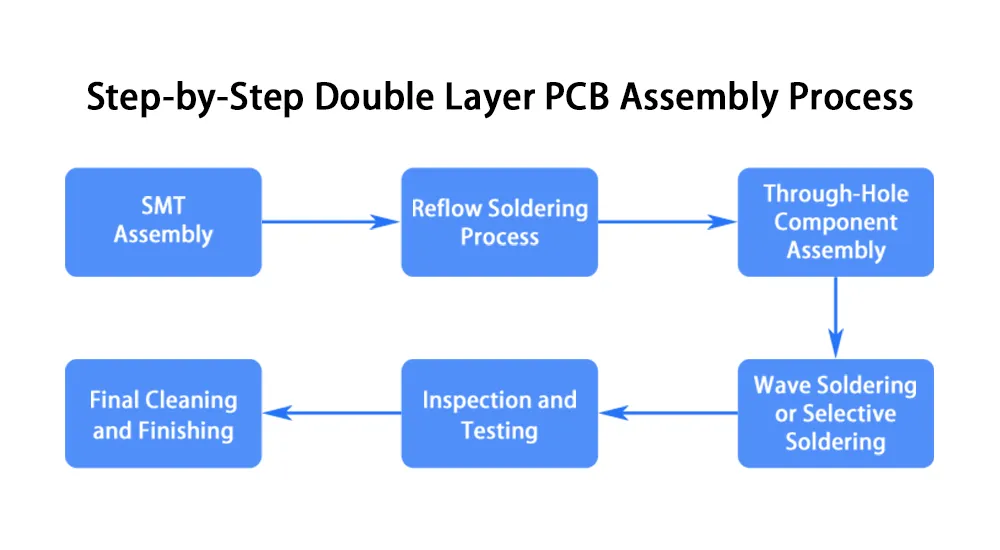
Step 1: Surface Mount Technology (SMT) Assembly
The double layer PCB assembly process begins with placing surface mount components on the primary side of the circuit board. This step requires accurate solder paste application using laser-cut stencils to ensure uniform paste volume and precise alignment.
Printing parameters—such as print speed, squeegee pressure, and separation speed—must be carefully calibrated based on the board design and component layout. High-precision pick-and-place machines then mount components, achieving placement tolerances within ±25 micrometers for fine-pitch packages.
SMT assembly typically follows a specific placement order, starting with small passive components and gradually progressing to larger integrated circuits. This sequence minimizes the risk of component shift and promotes proper solder joint formation during reflow.
Step 2: Reflow Soldering Process
Reflow soldering is a critical step that solidifies the electrical and mechanical connections of SMT components. It requires tightly controlled thermal profiling to ensure proper solder melting while avoiding damage to sensitive parts. Typically, the process uses a multi-zone convection oven with programmable heating and cooling stages.
| Reflow Phase | Temperature Range | Duration | Purpose |
|---|---|---|---|
| Preheat | 150-180°C | 60-90 seconds | Activate flux, evaporate solvents |
| Thermal Soak | 180-200°C | 60-120 seconds | Equalize board temperature |
| Reflow | 230-250°C | 30-60 seconds | Melt solder, form joints |
| Cooling | Below 200°C | 60-90 seconds | Solidify solder joints |
Proper temperature profiling ensures compatibility with component thermal limits while achieving complete solder reflow. In nitrogen-based reflow environments, oxygen levels should be maintained below 50 ppm to minimize oxidation and promote optimal solder wetting.
Step 3: Through-Hole Component Assembly
Once SMT reflow is complete, the assembly process proceeds to through-hole component insertion. This stage requires careful lead preparation and insertion techniques to avoid damaging previously mounted SMT components.
Through-hole assembly involves forming component leads to accommodate PCB thickness and spacing constraints. While automated insertion machines are suitable for standard parts, specialized or sensitive components may need manual handling for proper placement.
Retention methods—such as mechanical clinching, adhesive application, or temporary fixtures—are used to hold components in place during soldering. Precise lead trimming is also important to ensure clean solder joints and to avoid interference with adjacent components or board layers.
Step 4: Wave Soldering or Selective Soldering
Soldering of through-hole components typically involves either wave soldering or selective soldering, depending on assembly complexity and thermal sensitivity.
Wave soldering is ideal for high-throughput production, using molten solder waves to simultaneously form joints across multiple pins. Preheating stages and flux application help prepare the board for effective solder wetting and joint formation.
Selective soldering offers greater precision and thermal control, making it well-suited for mixed-technology assemblies where only specific through-hole components require soldering. This method minimizes thermal exposure to surrounding SMT components and supports tighter thermal profiles for double layer PCB assemblies.
Step 5: Inspection and Testing
Quality assurance is a critical part of the double layer PCB assembly process, involving both visual and electrical testing to verify assembly accuracy and functionality. Automated Optical Inspection (AOI) systems provide fast and detailed checks of solder joints, component placement, and polarity.
Key inspection criteria include solder fillet shape, correct orientation, and the absence of solder bridges. X-ray inspection is especially valuable for identifying hidden defects in Ball Grid Array (BGA) and other area-array packages.
Electrical testing methods such as In-Circuit Testing (ICT) help verify component values and signal continuity, while functional testing ensures the assembled board meets design specifications and operates as intended in its target application.
Step 6: Final Cleaning and Finishing
After all components are soldered and tested, final cleaning is performed to remove flux residues and other contaminants that may affect long-term reliability. The cleaning method depends on the flux type and board requirements.
Aqueous cleaning systems use deionized water with detergents to remove water-soluble fluxes, while solvent-based systems are preferred for rosin or no-clean fluxes. Ultrasonic cleaning may also be used for assemblies with tight spacing or complex geometries.
Final finishing steps may include the application of conformal coatings for environmental protection, additional electrical testing, and cosmetic inspections. Packaging should protect the boards from electrostatic discharge (ESD) and mechanical damage during shipping and storage.
Advanced Considerations for Double Layer PCB Assembly
Modern double layer PCB assembly increasingly incorporates advanced packaging technologies including fine-pitch components, embedded components, and rigid-flex configurations. These applications demand specialized assembly techniques and enhanced process control capabilities.
Thermal management considerations become critical in high-density double layer PCB assembly applications, requiring careful component placement strategies and thermal relief design optimization. Signal integrity requirements may necessitate controlled impedance considerations and electromagnetic interference (EMI) mitigation strategies.
Quality Assurance and Testing Protocols
Comprehensive quality assurance programs ensure consistent double layer PCB assembly results across production volumes. Statistical process control (SPC) methodologies enable continuous process optimization and defect prevention strategies.
Testing protocols should encompass both component-level and system-level validation, including boundary scan testing for complex digital assemblies and analog parameter verification for mixed-signal applications. Traceability systems enable comprehensive documentation of assembly genealogy and process parameters for regulatory compliance and continuous improvement initiatives.
Common Challenges and Solutions
Double layer PCB assembly presents unique challenges including component interaction effects, thermal cycling considerations, and rework complexity. Addressing these challenges requires systematic approach development and specialized equipment capabilities.
Tombstoning effects in SMT components can be mitigated through solder paste volume optimization and component placement force calibration. Thermal cycling stress management involves careful material selection and assembly process optimization to minimize coefficient of thermal expansion (CTE) mismatches.
Conclusion
The double layer PCB assembly process requires precision, expertise, and strict quality control to deliver reliable results in today’s competitive electronics market. Achieving success depends on a thorough understanding of assembly techniques, advanced equipment, and comprehensive quality assurance.
At Haoyue Electronics, we provide professional double layer PCB assembly services tailored to meet the most demanding specifications across a wide range of industries. Equipped with cutting-edge manufacturing facilities and an experienced engineering team, we ensure high-quality outcomes for both prototype and high-volume production projects.
Reach out to our technical experts today to discuss your assembly needs and learn how our expertise can help accelerate your product development while maintaining exceptional quality standards.
FAQ
1. What are the main steps involved in the double layer PCB assembly process?
The process typically includes surface mount technology (SMT) assembly on the primary side, reflow soldering, through-hole component insertion, wave or selective soldering, inspection and testing (including AOI and ICT), followed by final cleaning and finishing. Each step requires precise control to ensure reliability and performance.
2. How do manufacturers ensure quality during double layer PCB assembly?
Quality assurance is maintained through controlled environment conditions, component verification (including moisture sensitivity and orientation), solder paste quality checks, advanced inspection methods like Automated Optical Inspection (AOI) and X-ray inspection, plus rigorous electrical testing such as In-Circuit Testing (ICT) and functional validation.
3. What challenges are common in double layer PCB assembly, and how are they addressed?
Common challenges include component interaction effects, thermal cycling stresses, and rework difficulties. Solutions involve optimizing solder paste volume to reduce tombstoning, carefully selecting materials to minimize thermal expansion mismatch, and using specialized equipment and process controls to enhance assembly accuracy and durability.
4. What advanced considerations should be taken into account for high-density double layer PCB assemblies?
High-density assemblies often involve fine-pitch and embedded components or rigid-flex designs, requiring specialized assembly techniques. Critical factors include thermal management strategies, controlled impedance routing for signal integrity, and effective electromagnetic interference (EMI) mitigation to ensure optimal performance.

