Understanding Double Layer PCB Technology
Construction and Design Fundamentals
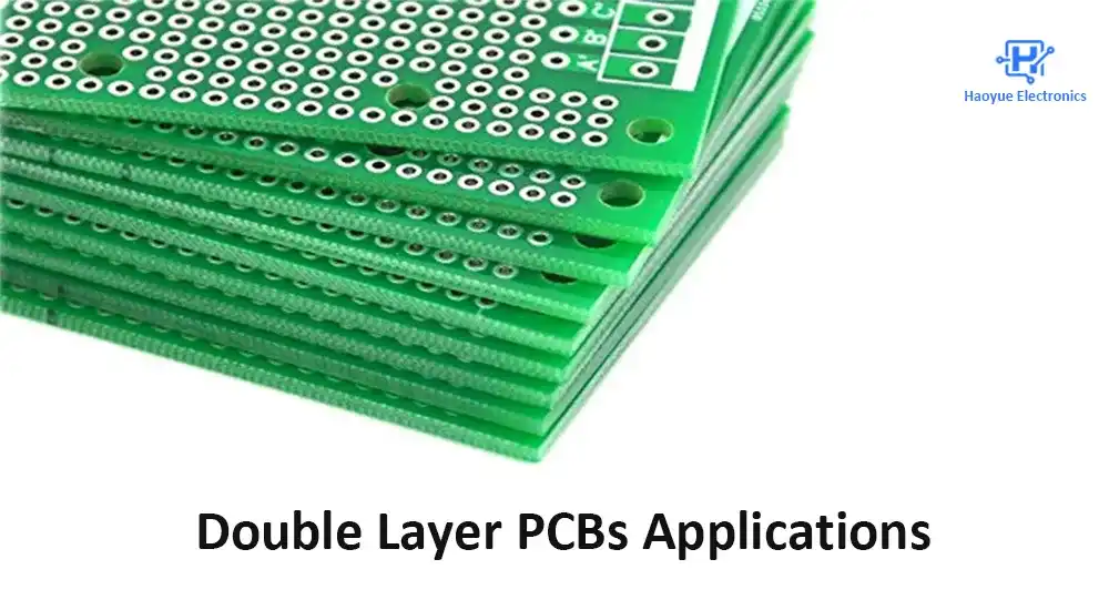
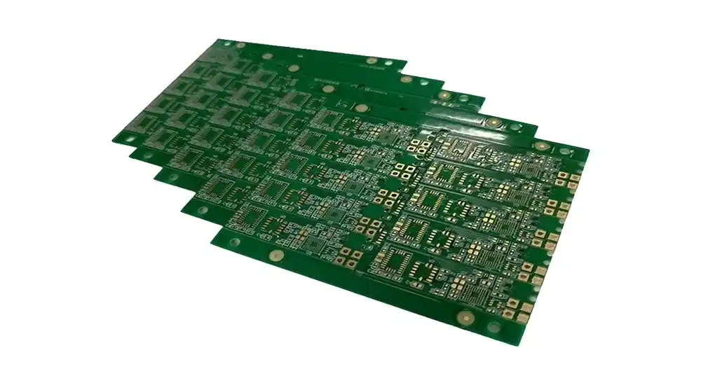
Double-layer PCBs, also known as two-layer PCBs, feature conductive copper traces on both the top and bottom surfaces of a dielectric substrate. This configuration doubles the available routing space compared to single-layer boards, enabling more complex circuit designs in compact form factors. The two copper layers are electrically connected through plated through-holes (PTHs) or vias, allowing signals to seamlessly transition between layers.
The substrate material, typically FR-4 fiberglass epoxy resin, provides mechanical stability and electrical insulation between the copper layers. Modern double-layer PCB manufacturing processes achieve trace widths as narrow as 0.1mm and via diameters as small as 0.2mm, supporting high-density interconnect designs crucial for modern electronic applications.
Key Technical Specifications
Double-layer PCBs typically operate within specific parameters that determine their suitability for different applications:
| Specification | Typical Range | Application Impact |
|---|---|---|
| Board Thickness | 0.8mm - 3.2mm | Mechanical constraints, connector compatibility |
| Trace Width | 0.1mm - 2.0mm | Current carrying capacity, signal integrity |
| Via Size | 0.2mm - 0.8mm | Design density, manufacturing cost |
| Copper Weight | 0.5oz - 2oz | Power handling, thermal management |
| Operating Temperature | -40°C to +130°C | Environmental application range |
Primary Double Layer PCB Applications Across Industries
1. Consumer Electronics Applications
Consumer electronics represent the largest market segment for double-layer PCB applications. These circuits power everyday devices that require reliable performance at competitive price points.
Smartphone and Mobile Device Components
Double-layer PCBs are essential for mobile devices, handling power management circuits, sensor interfaces, and auxiliary processing modules. Their compact design enables efficient use of internal space, ensuring signal integrity for high-frequency applications. They are commonly used in battery charging circuits, audio amplifiers, and camera interface boards.
Home Appliance Control Systems
Modern appliances increasingly rely on sophisticated control electronics. Double-layer PCBs are used for user interface panels, motor control circuits, and sensor integration in devices like washing machines, refrigerators, and HVAC systems. The cost-effectiveness of double-layer PCBs makes them ideal for mass production in appliance manufacturing.
Gaming and Entertainment Devices
In gaming controllers, audio equipment, and digital media players, double-layer PCBs are used for input processing, signal conditioning, and power distribution. These devices benefit from enhanced routing capabilities while maintaining compact designs, making them ideal for portable entertainment systems.
2. Industrial and Automotive Applications
Industrial environments require durable electronic solutions that can withstand tough conditions. Double-layer PCBs excel in such challenging applications.
Automotive Electronic Control Units (ECUs)
Modern vehicles contain multiple ECUs, controlling functions from engine management to infotainment systems. Double-layer PCBs handle sensor interfaces, actuator control, and communication protocols like CAN bus. Their reliable performance in extreme temperatures and vibration environments meets the rigorous standards of automotive manufacturing.
Industrial Automation and Control
In manufacturing equipment and robotics, double-layer PCBs support distributed control systems. These circuits handle analog sensor inputs, digital communication interfaces, and power switching functions, enabling smooth operation of automated systems. Their scalability allows them to serve both simple control modules and complex multi-axis motion controllers.
Power Electronics and Motor Drives
Variable frequency drives, power supplies, and motor control circuits often use double-layer PCBs to manage control logic and gate driver functions. The dual-layer structure provides effective isolation between high-voltage power circuits and low-voltage control electronics, all within a compact form factor.
3. Medical and Healthcare Devices
Medical electronics demand high reliability and must meet stringent regulatory standards. Double-layer PCBs support a range of healthcare applications where safety and performance are critical.
Diagnostic Equipment
Blood glucose meters, pulse oximeters, and portable diagnostic devices rely on double-layer PCBs for signal processing, data acquisition, and user interface functions. The reliable manufacturing process ensures compliance with medical device regulations.
Patient Monitoring Systems
Devices such as bedside monitors, telemetry systems, and wearable health trackers use double-layer PCBs for signal conditioning, wireless communication, and power management. Their long-term reliability and low power consumption make them ideal for healthcare applications.
4. Communications and Networking Equipment
The telecommunications sector extensively uses double-layer PCBs for both infrastructure and end-user devices.
Network Infrastructure Components
Routers, switches, and access points utilize double-layer PCBs for power distribution, LED indication circuits, and auxiliary processing. While high-speed data paths often require multilayer boards, many support circuits operate effectively with double-layer designs.
Wireless Communication Devices
Wi-Fi modules, Bluetooth interfaces, and IoT sensor nodes depend on double-layer PCBs for RF circuit implementation and digital processing. The controlled impedance properties of double-layer boards help maintain various wireless communication standards while keeping costs low in high-volume production.

Advantages and Technical Considerations
Performance Benefits
Double-layer PCBs offer significant advantages over single-layer alternatives while remaining more cost-effective than multilayer solutions. The dual copper layers provide improved electrical performance through better ground plane implementation and reduced electromagnetic interference. Signal integrity benefits from shorter trace lengths and dedicated return paths, which are essential for digital circuits operating at moderate frequencies.
The enhanced routing density enables more complex functionality within constrained board areas, directly supporting miniaturization trends in electronic devices. Power distribution capabilities improve significantly with dedicated power and ground layers, reducing voltage drops and enhancing overall system stability.
Cost-Effectiveness Analysis
Double-layer PCBs achieve an optimal balance between functionality and manufacturing cost. The production processes are well-established and widely available, ensuring competitive pricing for both prototypes and high-volume applications. Compared to multilayer alternatives, double-layer boards require fewer manufacturing steps, reducing production time and cost while maintaining adequate performance for many applications.
The maturity of the technology leads to predictable yields and reliable supply chains, both critical for commercial product development. Comprehensive design tool support is available, with most PCB design software packages offering robust capabilities for double-layer board development.
Design Limitations and Solutions
While double-layer PCBs offer significant advantages, certain limitations must be considered during the design phase. Layer count restrictions may require careful trace routing planning, especially for designs with high pin-count components or dense interconnections. Thermal management becomes more challenging compared to multilayer boards with dedicated thermal planes.
Design engineers can address these limitations through strategic component placement, via optimization, and thermal relief techniques. Modern design software provides automated routing capabilities that maximize the dual-layer routing potential while maintaining signal integrity requirements.
Manufacturing and Quality Considerations
Production Requirements
Double-layer PCB manufacturing requires precise control of several critical parameters. Copper plating thickness uniformity ensures consistent electrical performance across the entire board surface. Via plating quality is crucial for reliable interlayer connections and requires careful process control during electroplating.
Solder mask application and silkscreen printing must accommodate the dual-layer configuration while maintaining registration accuracy. Modern manufacturing facilities use automated optical inspection (AOI) and electrical testing to verify board quality before shipment.
Quality Standards and Testing
Double-layer PCBs must meet various industry standards depending on their intended applications. IPC-A-600 provides acceptability criteria for printed boards, while IPC-6012 specifies qualification and performance requirements. Automotive applications may require additional standards, such as IATF 16949 compliance.
Electrical testing typically includes continuity verification, insulation resistance measurement, and high-voltage isolation testing. For critical applications, additional tests like thermal cycling, vibration resistance, and accelerated aging may be required to ensure long-term reliability.
Ready to Transform Your Electronic Designs?
At Haoyue Electronics, we specialize in manufacturing high-quality double-layer PCBs that meet the demanding requirements of modern electronic applications. Our advanced production facilities and experienced engineering team ensure that your projects receive the precision manufacturing and technical support they need for success.
Whether you’re developing consumer electronics, industrial controls, or medical devices, our comprehensive PCB assembly services provide the reliability and performance your applications demand.
Contact our technical team today to discuss how our double-layer PCB solutions can optimize your next project’s performance and cost-effectiveness.
Frequently Asked Questions about Double Layer PCBs
1. What is a Double Layer PCB and what are its advantages?
A Double Layer PCB, also known as a two-layer PCB, features copper traces on both the top and bottom surfaces of the substrate material. Compared to single-layer PCBs, it provides more routing space and enables more complex circuit designs. The dual-layer structure improves signal integrity, reduces electromagnetic interference, and is more cost-effective than multilayer PCBs. It is widely used in consumer electronics, automotive, medical devices, and telecommunications.
2. Which industries are best suited for Double Layer PCBs?
Double Layer PCBs are widely used in various industries, including:
- Consumer Electronics: Smartphones, home appliances, gaming devices, etc.
- Industrial & Automotive: Automotive ECUs, industrial automation, power electronics, and motor drives.
- Medical & Healthcare Devices: Blood glucose meters, bedside monitors, and wearable health devices.
- Communications & Networking: Routers, switches, Wi-Fi modules, Bluetooth interfaces, etc.
3. What are the primary performance benefits of using Double Layer PCBs?
Double Layer PCBs provide several performance advantages over single-layer alternatives:
- Improved Electrical Performance: The dual copper layers provide better ground plane implementation, reducing electromagnetic interference (EMI).
- Enhanced Signal Integrity: Shorter trace lengths and dedicated return paths lead to higher signal quality, particularly important in high-frequency applications.
- Miniaturization Support: Increased routing density enables more complex functionality within smaller board spaces, supporting the miniaturization trends in electronic devices.
- Better Power Distribution: Dedicated power and ground layers reduce voltage drops and enhance overall system stability.
4. What are the key production requirements for Double Layer PCB manufacturing?
Double Layer PCB manufacturing requires precise control of several critical parameters to ensure board quality:
- Copper Plating Uniformity: Ensures consistent electrical performance across the entire board.
- Via Plating Quality: Critical for reliable interlayer connections.
- Solder Mask & Silkscreen Printing: Must accommodate dual-layer configuration while maintaining accuracy.
- Automated Optical Inspection (AOI) & Electrical Testing: Ensures board quality before shipment.
5. How can design limitations of Double Layer PCBs be addressed?
Although Double Layer PCBs offer many advantages, certain limitations need to be considered during the design phase, such as layer count restrictions and thermal management issues. These limitations can be addressed by:
- Optimizing Component Placement: To minimize trace lengths and improve signal integrity.
- Optimizing Via Design: To increase design density and reduce manufacturing costs.
- Utilizing Thermal Relief Techniques: To address thermal management challenges and ensure stability.

